Oxygen plasma patterning technique forms optical metasurfaces that remain planar

In a development that could benefit the burgeoning field of infrared (IR) thermal-control coatings, researchers from the University of Southampton (England) have demonstrated a new fabrication technology that can create high-quality nanostructured optical metasurfaces for IR thermal control coatings and nonlinear optics using plasma patterning.1
Conventional methods of producing optical metasurfaces take place in specialized cleanroom facilities (such as the Southampton Nanofabrication Centre), where patterns are etched into materials or separated structures are deposited on the surface using lift-off lithography. However, the resulting surface topography is often undesirable and can strongly limit the device performance when embedded into a stack of many independent layers.
In their study, the Southampton researchers explored a new technology that locally and selectively modulates optical properties without changing the flatness of the material surface. The research team based their new technique on the discovery that an oxygen (O2) plasma can greatly reduce the electron (carrier) concentration of certain transparent conducting oxides (TCOs) such as indium tin oxide (ITO) and aluminum (Al)-doped ZnO (AZO).
Transparent conductive oxides such as AZO have a high electron density, making them dielectric in the visible range, but metallic in the IR. This electron density of AZO is critical for its material electrical and optical properties. Ordinarily, to achieve an optical property contrast by spatially varying the carrier concentration, which is required for optical metasurface formation, parts of the AZO film needs to be removed, leaving a nonplanar structure. The Southampton researchers can now achieve the same thing via their new O2 plasma treatment; because the treatment maintains planarity of the layer, further optical layers added to the structure (to produce a finished metasurface) are not affected by undesired surface topography. The control of the O2 plasma is made possible by accurate location control through lithographic location definition.
MWIR and LWIR versions
In one experiment, a 100-nm-thick AZO film was deposited on a calcium fluoride (CaF2) substrate using thermal atomic-layer deposition (ALD), then exposed to a 300°C O2 plasma for treatment times of up to 20 minutes. The initial carrier density of 2.7 × 1020 cm−3 was reduced to below 5 × 1019 cm−3 (the sensitivity limit of the experiment), with the two resulting carrier densities well suited for optical metasurfaces in the longwave-IR (LWIR) at wavelengths greater than 8 μm. In addition, the researchers fabricated a different AZO film with an increased optical carrier density of 6 × 1020 cm−3, a density suitable for midwave-IR (MWIR) applications at wavelengths less than 10 μm, and then applied their O2 plasma treatment, reducing the carrier density in a similar way to that of the LWIR treatment. The carrier-density reduction in the MWIR version resulted in a visible-range transmission of 70%, along with high transmission in the near-IR and IR ranges.
The researchers also fabricated two different metasurfaces using O2 plasma or conventional etching, with 700 nm features and 250 nm gap. IR emissivity, which is an indicator of how well the surfaces might perform as thermal control coatings, agreed well for the metasurfaces fabricated using the two different techniques, showing the efficacy of the O2 plasma approach (no additional coatings were deposited atop the metasurfaces for the experiment).
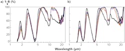
In addition, a multiband metasurface with silver plasmonic features on an AZO metasurface was created (see figure). In this configuration, the fabrication of the silver plasmonic antennas was benefited by the fact that the AZO metasurface below was planar.
“Plasma patterning provides a completely new route to form electrical and optical devices with structures beyond existing manufacturing limitations,” says Kai Sun, one of the researchers. “Here, we have shown for the first time that a planar metasurface, based on aluminum-doped zinc oxide, can be achieved with an optical metasurface function, but physically flat. The metasurface devices in this work are only a start of this new technique’s applications and its full potential impact is still to be seen.”
The study found that oxygen plasma can reduce Al:ZnO electron density by up to five orders of magnitude. This led the team to propose the new fabrication technique that forms a metasurface by selectively modulating the electron density using oxygen plasma, made possible by accurate location control through a lithography definition.
The Southampton researchers have applied for a UK patent on the O2 plasma patterning technique.
REFERENCE
1. K. Sun et al., Adv. Mater. (2020); https://doi.org/10.1002/adma.202001534.
About the Author
John Wallace
Senior Technical Editor (1998-2022)
John Wallace was with Laser Focus World for nearly 25 years, retiring in late June 2022. He obtained a bachelor's degree in mechanical engineering and physics at Rutgers University and a master's in optical engineering at the University of Rochester. Before becoming an editor, John worked as an engineer at RCA, Exxon, Eastman Kodak, and GCA Corporation.
