IR Optics: Femtosecond laser polishing could be new approach for figuring germanium optics

Precision freeform optics can be polished in several ways, including traditional polishing, belt polishing, and magnetorheological finishing (MRF), and others. Now, an additional approach may be added to the mix: laser polishing—at least if the optics to be finished are germanium (Ge). Optics made of Ge are potentially useful not only for small-batch precision infrared (IR) optics for defense, but could also, if made in large-enough quantities, serve as optics for smartphone-based optical systems for industry and possibly even for consumers (in the form of thermal imagers for mapping heat loss in houses, for example).
A group of researchers from the University of Rochester and the Rochester Institute of Technology (both in Rochester, NY) and Aperture Optical Sciences (Meriden, CT) is now experimenting with femtosecond lasers for near-nonthermal polishing and figuring of Ge optics especially as a method for preventing the mid-spatial-frequency figuring errors that are common with existing freeform-optics polishing techniques.
Minimal thermal effects
As the researchers note, femtosecond lasers can be focused to gigawatt to terawatt per square centimeter intensities, which lead to very spatially precise material removal with minimal thermal effects. The researchers’ efforts went toward preventing significant melting, oxidation, and gas bubble and ripple formation during the laser-based material removal by carefully optimizing the experimental conditions.
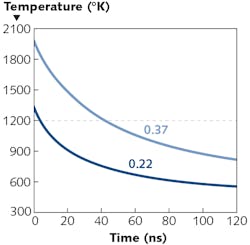
Before the actual experiments, a 3D so-called two-temperature model (TTM) was created to simulate the laser-based material removal of Ge that included the transferral of heat to free-carrier electrons that then collide with and transfers heat to the Ge material lattice until the system reaches thermal equilibrium. For example, TTM results were calculated at the material surface and the center of the incident Gaussian pulse for two different peak fluences of 0.37 and 0.22 J/cm2 (see figure). The calculation showed the onset of ablation and rise in electron-system temperature to 2.9 × 10⁴ K for a fluence of 0.37 J/cm2 and 1.6 × 10⁴ K for a fluence of 0.22 J/cm (exceeding the Ge melting temperature of 1213 K).
The researchers designed the system so that there was enough time between pulses that the Ge surface could return to near its initial temperature before the next pulse. The repetition rate and scan speed could be controlled up to 2 MHz and 4 m/s, respectively, with a repetition rate on the order of 100 to 500 kHz and a scan speed on the order of 1 to 4 m/s considered optimum.
The experiment started with Ge substrates with a <111> crystal orientation and an approximately 1 nm root-mean-squared (RMS) surface roughness, which were processed using a 300 fs, 1030 nm ytterbium fiber laser having a 1/e2 laser focal-spot radius of 30 μm, which was scanned across the Ge specimen. In one experimental run, a region of Ge surface about 0.5 × 0.5 mm in size was polished with line overlap set to 75% of the laser focal-spot diameter. Scratches and discoloration disappeared due to the processing, as measured using a Zygo NewView imager.
Full-area height maps showed that the laser polishing effectively removes surface defects while maintaining subnanometer surface roughness, which confirms the capability of femtosecond laser polishing for high-precision material-removal tasks where 4 to 30 nm of material was removed.
REFERENCE
1. L. L. Taylor et al., Opt. Mater. Express (2019); https://doi.org/10.1364/ome.9.004165.
About the Author
John Wallace
Senior Technical Editor (1998-2022)
John Wallace was with Laser Focus World for nearly 25 years, retiring in late June 2022. He obtained a bachelor's degree in mechanical engineering and physics at Rutgers University and a master's in optical engineering at the University of Rochester. Before becoming an editor, John worked as an engineer at RCA, Exxon, Eastman Kodak, and GCA Corporation.
