3D-printed Optics: Focused femtosecond pulses print optical components with subdiffraction-limited resolution
![FIGURE 1. HP3DP provides scalability in size, complexity, shape, and processing substrate, as shown by the following SEM images: Submicrometer structures randomly oriented (a); micrometer-sized pyramidal structures with defined angles for light guidance (b); a macrostructure consisting of a 1 mm lens embedded into a frame with integrated assembly features (c); stacked microlenses fabricated in a single process step (for demonstration, the design was partially clipped to display the different elements [d]); a 1 x 1 cm lens array as a master for replication production (e); and a cylindrical microlens for beam-shaping purposes that was printed directly on the laser facet of an edge-emitting DFB laser ([e]; DFB laser from the company nanoplus).](https://img.laserfocusworld.com/files/base/ebm/lfw/image/2019/12/1912LFW_ste_f1.5de8074b6f8c1.png?auto=format,compress&fit=fill&fill=blur&q=45?w=250&width=250)
BENEDIKT STENDER, FABIAN HILBERT, JONAS WIEDENMANN, ALEXANDER KRUPP, WILLI MANTEI, and RUTH HOUBERTZ
As one of the enabling technologies in the 21st century, 3D printing has gained popularity in rapid prototyping and manufacturing because only one process step is necessary—in addition, the process does not require expensive and elaborate production of conventional tooling. 3D printing not only provides fast evaluation of prototypes, but also can enable more-efficient low- to medium-volume production compared to traditional manufacturing. In many cases, the 3D-printed parts may weigh less and offer improved overall mechanical stability compared to conventionally assembled parts. Although many applications have been demonstrated, due to low precision and lack of suitable materials, the printing of elements with optical functionality remains impossible. However, by providing submicrometer printing resolution via nonlinear absorption of two photons simultaneously triggered by focused femtosecond laser pulses, high-precision 3D printing (HP3DP) aims to deliver real 3D printing with resolution on demand. By focusing laser pulses in a vat of special polymers or glasses, two- or multiphoton absorption effects create solid objects with a fidelity defined by the focal spot of the laser. Compared to repetitive 2D layer-by-layer workflows characteristic of most other 3D printing technology, the HP3DP process is not only additive, but can also be subtractive, as the focal spot can create surface effects in solid objects as well.
Bridging the gap between micro/nanofabrication and conventional fabrication technologies, the HP3DP process creates components at a resolution below the diffraction limit that are scalable in overall size from the submicron to the centimeter range. The ability to fabricate structures with aspect ratios as high as 43:1 and control the focal volume for rapid production runs enables the printing of ultrahigh-quality micro-optics, microfluidic devices, and other components not possible using conventional machining methods.
Printing resolution and scalability
Since the effect of HP3DP was first demonstrated in 1997,2 it has evolved steadily due to the participation of many academic and research group investigations. The technique has matured to the point where high-printing-resolution industrial applications are possible. Resulting from the nonlinear absorption effect spatially confined to the focal volume and its probability to the square of the applied laser power, feature sizes below the diffraction limit are possible at the 100 nm range.3 The size of the smallest features, called voxels, used to build up larger elements can be instantaneously adjusted by the laser power, the focusing optics, the fabrication strategy, and the processed material itself.
This direct laser writing method provides a high degree in scalability with respect to size, complexity, structured area, and substrate processability enabled by the corresponding fabrication throughput and the fact that the digital data preprocessing does not rely on expensive masks (see Fig. 1). An example illustrates scalability in size (see Fig. 1a) for submicrometer structures in arbitrary arrangements and shapes to microstructures (see Fig. 1b) and macrostructures (see Fig. 1c) with a large lens (one millimeter in diameter) integrated into a box with alignment features.
Because HP3DP provides real 3D fabrication, complex structures such as a stacked microlens array (see Fig. 1d) can be fabricated in a single process step without alignment of the individual elements with respect to each other—a challenging job with high sensitivity to malfunction of the final device in traditional manufacturing of endoscopes.
For mass manufacturing, large-area fabrication is necessary. Via implementation of sophisticated manufacturing strategies,4 HP3DP can be used for suitable master fabrication of lens arrays for wafer-scale optics such as ultraviolet and step-and-repeat nanoimprint lithography, as shown for a 1 × 1 cm2 array (see Fig. 1e), or for the fabrication of replication molds for other mass-manufacturing technologies such as injection molding and hot embossing.
Additionally, depending on the corresponding fabrication design, direct mass manufacturing is also possible. Contrary to other 3D printing technologies, HP3DP does not require wiping steps for deposition of new/fresh material within the layer-by-layer based process. Therefore, there is no limitation on special substrates (see Fig. 1f)—for example, where a microlens was printed directly on the facet of an edge-emitting distributed-feedback (DFB) laser from nanoplus (Gerbrunn, Germany) to compensate for the elliptical beam shape originating from the difference of divergence along the so-called fast and slow axes.
While typically, bulky macro lenses are applied to achieve a spherical beam profile, this unique ability to print elements on any interface, including active devices and passive devices like waveguides, fibers, and detectors, enables a high degree of flexibility in designing new miniaturized products and packaging concepts, as well as the possibility of combining several laser wavelengths at a single output (combiner) for lab-on-chip applications.
High-aspect-ratio structures
For microelectromechanical applications, high-aspect-ratio (HAR) structures are favorable because they enable 3D microelectromechanical system (MEMS) structures. Such MEMS structures are typically processed via LIGA (a German acronym for Lithographie, Galvanik and Abformung), which mainly uses SU-8 photoresist and chrome masks. The process requires several process steps, including the challenging task of casting thick photoresist layers typically limited to a few hundreds of microns. Consequently, for a height of 100 µm, a HAR of 100:1 has been realized. However, larger vertical dimensions pose a fabrication challenge due to the requirement of thicker resist-layer deposition.
In contrast, a typical HP3DP exposure mode focuses laser pulses on a liquid photoresist that is contained in a vessel with depths ranging from several millimeters to centimeters. Container depth is limited by the working distance of the microscope’s objective in the case of top-side illumination, and when illuminating from the bottom, depth is limited by the traveling distance of the motion axis. The result is that the printing height is easily varied up to the centimeter range. Another factor to consider when realizing HAR structures with vertical dimensions >100 µm is the material’s stability. The HP3DP generally exposes a liquid photoresist material such as ORMOCERs, an inorganic-organic hybrid polymer with glasslike properties in terms of transmission and hardness.
Typical HAR structures realized by HP3DP (see Fig. 2) include waveguides with aspect ratios of 1:1 or 2:1—HAR structures of 16:1 with 90° side walls are shown. Long walls 5 µm wide and 80 µm high were fabricated in an infinite field-of-view (IFoV) mode, comprising a synchronized laser focus deflection by the galvo scanner and the traveling range. This structuring mode enables stitchless fabrication of elements larger than the microscope objective’s field of view (FoV). In this particular example, the length was 4X larger than the FoV of the microscope objective. HAR structures of 20:1 are even possible. For example, 100-µm-high needles with 5 × 5 µm2 base area can be used for local light stimulation of living cells by guiding the light from a source to the living specimen, or as cantilevers in atomic-force microscopy for the evaluation of challenging topographies.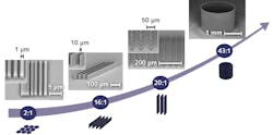
Contouring is also possible. The process involves first crosslinking via laser processing the enclosed liquid photopolymer, then washing away the unexposed material in a subsequent step until the corresponding shell of the object is all that remains. After developing, a UV flash is applied to polymerize the confined inner resist to achieve a homogeneous crosslinking between shell and core. With this method, a tremendous enhancement of fabrication throughput by up to 95% compared to conventional full-volume structuring mode was demonstrated in the serial manufacturing of microlenses, achieving only 1–5 s per lens.5
A corresponding HAR structure of 43:1 is illustrated (see upper right upper position of Fig. 2) for a cylinder-like element with a height of 1.7 mm and a diameter of 2 mm. In an analogous manner as described above, the cylinder was structured using an IFoV structuring mode with a circular movement of the linear translation stage accompanied by a radial deflection of the laser focus, or so-called railroad beam steering (RBS). For demonstration purposes, the cap has not been processed to show the 0.04 mm wall thickness. The fabrication throughput for this type of structure was 3.6 mm3/h and can be even further enhanced using laser-beam-shaping tools such as splitting or top-hat generation.
It must be mentioned that the demonstrated aspect ratio of 43:1 is not the upper limit. The displayed microstructures are just a few cases serving as illustration examples and were not explicitly addressed for HAR demonstration. Using optimized design generation, even with submicrometer lateral dimensions, higher aspect ratios are possible.
Summary
Due to its high printing resolution and scalability in size, complexity, shape, and processing substrate, the HP3DP process will be increasingly applied in industrial applications. Because the HP3DP process enables creation of components with resolution below the diffraction limit that are scalable in overall size from the submicron to the centimeter range, 3D printing of optical quality surfaces in micro-optical applications is the main application area. The ability to fabricate structures with aspect ratios as high as 43:1 and control the focal volume for rapid production runs results in ultrahigh-quality micro-optics, microfluidic devices, and other components not possible using conventional machining methods.
REFERENCES
1. X. Zhou et al., AIP Advances, 5, 3 (2015).
2. S. Maruo et al., Opt. Lett., 22, 2, 132–134 (1997).
3. S. Steenhusen, “Untersuchungen zur sub-100 nm Strukturierung von Hybridpolymeren mittels Zwei-Photonen Absorption und Anwendungen,” Friedrich-Schiller-Universität Jena (2018).
4. B. Stender et al., Adv. Opt. Technol., 8, 3–4, 225–231 (2019).
5. B. Stender et al., Laser Tech. J., 14, 2, 20–23 (2017).
Benedikt Stender is CTO; Fabian Hilbert, Jonas Wiedenmann, Alexander Krupp, and Willi Mantei are application engineers; and Ruth Houbertz is CEO and managing director, all at Multiphoton Optics, Würzburg, Germany; e-mail: [email protected]; https://multiphoton.net.