Imec extends silicon photonics portfolio targeting next-generation datacenter interconnects
At the 45th European Conference on Optical Communication (ECOC; 22-26 Sept. 2019) held this week in Dublin, Ireland, Imec (Leuven, Belgium), together with IDLab and the Photonics Research Group, both Imec research labs at Ghent University, are presenting their milestone results in silicon photonics (SiPho) technology development. The demonstrated building blocks help pave the way for 400 Gbit/s and beyond optical links as well as for copackaged optics in next-generation datacenter switches.
Highlights include a through-silicon-via (TSV)-assisted, high-density (Tbit/s/mm2) CMOS-SiPho transceiver prototype, a low-power 106 Gbit/s PAM-4 SiPho transmitter, a high-speed germanium/silicon (Ge/Si) avalanche photodetector, and ultrabroadband low-loss single-mode fiber couplers.
In the next few years, datacenter optical links will be upgraded to 400 Gbit/s capacity by aggregating four 100 Gbit/s PAM-4 lanes per link. As a consequence, the aggregate bandwidth to be handled by a single datacenter switch will increase to 51.2 Tbit/s, requiring ultrahigh-density SiPho transceiver technology tightly integrated and copackaged with the switch CMOS chip.
200 and 300 mm wafers
To help industry to meet these challenging scaling requirements, Imec and its research labs at Ghent University are developing technology building blocks by using Imec’s Si photonics platforms on 200 mm and 300 mm wafers in combination with high-speed electronics. “Our R&D programs have delivered substantial improvements at various levels of Si Photonics technology, both at the level of process integration, individual component development as well as at the subassembly level,” Joris Van Campenhout, Program Director Optical I/O at Imec.
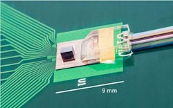
One of the highlights that Imec presents at ECOC is the first TSV-assisted hybrid FinFET CMOS/Si-photonics transceiver technology. Operating at a data rate of 40 Gbit/s non-return-to-zero (NRZ, single lane), this prototype combines ultralow power consumption with 1 Tbit/s/mm2 bandwidth density, paving the way to ultradense copackaged optics in future datacenter switches.
Imec and Ghent University are also presenting a 106 Gbit/s transmitter that uses PAM-4 as a modulation format. This four-level modulation format has recently been adopted by industry as the modulation format of choice for 53 GBd single-lane transmission over 500 m. Compared to other PAM-4 transmitters, Imec’s approach does not use any equalization or digital signal processing and integrates two parallel GeSi electroabsorption modulators. This results in a very compact and low-power (1.5 pJ/bit) transmitter able to transmit data over 1 km single-mode fiber at 106 Gbit/s.
Also, Imec demonstrates improved edge-coupler designs based on a hybrid Si/SiN photonic platform. Improvements to the layer stack resulted in better than -1.5 dB/fiber coupling efficiency to industry-standard single-mode fibers for operation in the O- and C-bands. On the receive side, a high-speed Ge/Si avalanche photodetector is presented with a multiplication gain of 8 and 32 GHz bandwidth. These avalanche photodetectors show potential for improving receiver sensitivities and optical link margins at data rates of 40 Gbit/s and beyond.
Source: Imec
About the Author
John Wallace
Senior Technical Editor (1998-2022)
John Wallace was with Laser Focus World for nearly 25 years, retiring in late June 2022. He obtained a bachelor's degree in mechanical engineering and physics at Rutgers University and a master's in optical engineering at the University of Rochester. Before becoming an editor, John worked as an engineer at RCA, Exxon, Eastman Kodak, and GCA Corporation.

