Advances in Optical Communications: Making optical printed circuit boards on an industrial scale
Glass, a unique material with several thousand years of history, is present in many parts of daily life. Now, as photonics evolves, glass is becoming even more important as a waveguiding material for light. In the last two decades, glass fibers have replaced metal wire for high-speed data transmission. In the move from purely electronic data processing towards photonics-enabled data processing systems, glass has the potential to take over data transmission on the printed circuit board (PCB), at the chip level, and in between.
The Fraunhofer Institute for Reliability and Microintegration IZM (Fraunhofer IZM; Berlin, Germany) is following this technological path. Founded 26 years ago to push the miniaturization and integration of electronic components forward, Fraunhofer IZM is now looking for new ways to integrate photonic data-processing technology into ever-smaller and more-complex structures to handle the growing volume and rates of data.
From electrons to photons
Current technological trends such as big data processing, global social-media networks, and the Internet of Things (IoT) require advanced processing structures. The rise of photonic integrated circuits and even quantum computers based on light leads to the question of how to connect these optical processing units.
For long-distance transmission, glass fibers are certainly a good solution. But for short distances, such as inside devices, this approach leads to a chaos of wiring similar to what could be found in electrical devices from the first half of the last century. The solution for electrical wiring chaos was the introduction of printed electrical connections, later known as printed circuit boards (PCBs).
In any case, the move from electronic to photonic data processing is not a one-to-one copying process. The table gives a rough overview of the required technological building blocks, including devices for creating, processing, transmitting, and receiving light, as well as electro-optic conversion and transceiver technology.
The colors in the table refer to technologies for aiding integration such as packaging (yellow) and silicon photonics (orange). It should be noted that the process of building a roadmap for photonic integration is ongoing—experts expect a new updated version for 2019. It is clear that the range of different photonic integration technologies is wide and goes far beyond what can be discussed in a single article.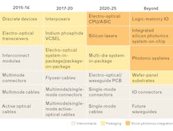
High bandwidth through integrated optical structures
Integrated circuits have grown over the years, not only in the number of transistors but also in physical size. But chips cannot be made larger without limit, as the yield in chip manufacturing becomes lower with increasing size. Thus, electronic chips get separated into subprocessing units on chiplets. Some of these are located on interposers, which are an intermediate carrier of chiplets with integrated data-transfer structures. The interposer may have horizontal or vertical connections with electrical or optical connections (or even both).
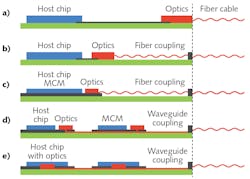
Ever-increasing data rates in communications between electrical processing units is causing physical limits to be reached. Optical connections between chips, interposers, and boards are considered a viable alternative for fast data transfer. Such an approach requires optical input-output (IO) units and, as a result, there is a need for further integration of optical interconnects (see Fig. 1). Optical transmission in circuit boards is highly desirable to avoid the wiring chaos problem.
Photonics functionality in thin glass
By changing the perspective from electrical printed circuit board to a photonic solution, the idea of the electro-optical circuit board (EOCB) was created. Driven by the need for higher bandwidth, the EOCB concept brings some ideas of the old electrical world into the design of new photonic structures. For example, an EOCB should have a light-conducting layer that takes over the task of data transfer. And of course, EOCBs need to fulfill a number of general requirements, with low cost, reliability, and easy manufacturability being most important.
There are two obvious choices for the material for the light-conducting layer—structured polymer layers as known from polymer optical fibers (POFs) and thin glass as known from displays. A waveguide in glass has higher transmission at telecom wavelengths and is more durable and less capable of thermal loads. Thanks to the rapid development of cell phones, thin glass is a viable alternative with high quality at low prices.
Instead of printed metal circuits, light is conducted in optical waveguides, which can be integrated by ion exchange within thin glass sheets. The material and the technology are compatible with silicon photonics and fiber optics and show high long-term stability, remaining reliable even at high thermal loads. Processing such material is an established process and making EOCBs of 305 mm × 440 mm is feasible.
Glass has two properties that are of particular interest for combination with conventional electronics: It is an excellent insulator, so direct contact with conductors is no problem. Unfortunately, glass has a very low thermal conductivity, so it is not suited for heat transport and thermal management has to be considered in the design.
The structure of an EOCB
To build up an EOCB, the glass sheets can be laminated with conventional organic base material such as FR4. Two different structures can be used together: Glass can be a core layer inside the conventional PCB base material (glass core), and glass can be used as the main carrier (a photonic interposer carrying all the PIC and electronic chip components). Copper can be plated on the glass and the organic material. The processing is compatible with regular PCB processing, but needs high-precision assembly.
Figure 2a shows the structure of a typical EOCB. The blue layer in the EOCB denotes a glass layer with integrated single-mode optical waveguides. The electrical processor is located on a glass interposer with a cooling surface on top. A critical point is the connection between the transceiver and the glass layer. Structuring through-glass electrical vias (TGVs) is an established process, but steering the photonic signals is the challenge. Currently, there are at least two techniques under development—either a periscope placed from the top or a small mirror positioned from the bottom of the EOCB. The industry has not yet established standards or multisource agreements for either of these techniques.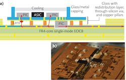
Several different design issues have to be solved for such an EOCB. These include electrical, where RF and electrical signal transmission need path optimization and signal-reflection removal; optical, where signal optimization, free-space collimation, and optomechanical system design must be considered; and thermal, where heat sources have to be regarded and sinks have to be integrated if necessary.
The result of such efforts is shown in Figure 2b. This is a fully operational photonic interposer for an onboard optical transceiver with 25 Gbit/s/ch transmission. A galvanic wafer-level process has been used for making TGVs. On the bottom side of the interposer, polymer lenses have been placed at the ends of the vertical optical pathways in glass—these collimate the light from vertical-cavity surface-emitting lasers (VCSELs) or other light sources on top of the interposer into free space. These signals can be captured by a deflecting mirror element on the underlying structure.
The system shown has very low optical losses of 0.5 dB in the receiver and <2 dB loss measured over a 2 mm distance from the polymer microlens on the transmitter side.
Making waveguides in display glass
An essential technology for EOCB is the fabrication of waveguides in the glass layer, which can be seen as the optical analog to printing circuits on a PCB. Waveguides can be tailored for single-mode (SM) or multimode (MM) transmission. While many datacom structures are working with multimode signals, silicon photonics is mostly based on the use of single-mode signals, which will be the focus of the following.
Waveguides in glass can be produced by lasers or by other technologies such as ion-exchange processes that originate from semiconductor processing. The latter have the advantage of parallel processing, while laser processes are inherently sequential because the laser has to follow the path of the waveguide.
The thermal (silver) ion-exchange process is well established for the creation of waveguides at a wafer level. At Fraunhofer IZM (Berlin, Germany), this procedure for integrated optics has been transferred to full panel level at sizes up to 610 mm × 440 mm. It has also been modified from a reliance on special glasses towards the use of cost-effective display glass. The whole process has been configured for large-scale manufacturing.
The process involves several steps as shown in Figure 3. First, an aluminum (Al) layer is sputtered on the glass surface. Next, a lithographic process removes the Al over all regions where waveguides have been designed. In a third step, the panel is immersed in hot molten-salt containing silver nitrate (AgNO3). The silver ions diffuse into the glass and replace sodium (Na) ions there, increasing the local index of refraction and creating a graded-index waveguide precursor.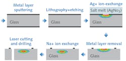
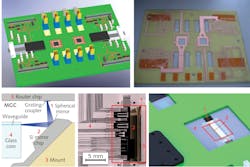
In a next step, the optical connectors have to be introduced. Such connectors are not standardized yet, but they either use a periscope or (curved) micromirrors to steer the signal from the interposer downwards to the horizontal EOCB waveguide layer (see Fig. 4, bottom). Such elements are aligned semiautomatically or in a fully automated manner using procedures that were developed for telecom equipment.
What is there, and what is missing?
Electro-optical circuit boards will be essential for effective data processing in the years to come. A substantial requirement is the development of integrated optical connections between electrical or photonics processing and storage units on various levels, from chips and chiplets via interposers up to full panels. Waveguides fabricated using an ion-exchange process in cheap display glass laminated with conventional PCB materials can solve this task. These processes have been scaled to a full-panel size of 610 mm × 440 mm, and the entire process chain is ready for transfer into large scale manufacturing, preferably in established PCB manufacturing lines.1 Many challenges remain—for example, several solutions have been developed for the alignment of connectors in TGVs, but no standard has been settled on yet.
REFERENCE
1. H. Schröder, M. Neitz, and M. Schneider-Ramelow, Proc. SPIE, 10538, 105380D (Feb. 22, 2018); doi:10.1117/12.2297363.
About the Author

Andreas Thoss
Contributing Editor, Germany
Andreas Thoss is the Managing Director of THOSS Media (Berlin) and has many years of experience in photonics-related research, publishing, marketing, and public relations. He worked with John Wiley & Sons until 2010, when he founded THOSS Media. In 2012, he founded the scientific journal Advanced Optical Technologies. His university research focused on ultrashort and ultra-intense laser pulses, and he holds several patents.
Henning Schröder
Head, Department for Optical Interconnection Technology at Fraunhofer IZM
Henning Schröder is head of the department for optical interconnection technology at Fraunhofer IZM (Berlin, Germany).