EVG & SCHOTT partner on 300 mm NIL wafers for AR/MR components
EV Group (EVG; St. Florian, Austria), supplier of wafer bonding and lithography equipment for the MEMS, nanotechnology, and semiconductor markets, has teamed up with specialty glass and glass ceramics company SCHOTT (Mainz, Germany) to demonstrate the readiness of 300 mm (12 inch) nanoimprint lithography (NIL) for high-volume patterning of high-refractive index (HRI) glass wafers used in the manufacture of waveguides/light guides for next-generation augmented/mixed reality (AR/MR) headsets.
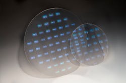
The partnership involves EVG’s proprietary SmartNIL process and SCHOTT RealView high-refractive index glass wafers and will be carried out within EVG’s NILPhotonics Competence Center at the company’s headquarters in Austria. SCHOTT will showcase a 300-mm SCHOTT RealView glass wafer patterned with EVG’s SmartNIL technology at the China International Optoelectronic Expo (CIOE), to be held September 4-7 at the Shenzhen Convention Center.
“Scaling up to 300-mm manufacturing of high-refractive index glass wafers is critical to achieving the production volumes at the economies of scale that our customers need to meet growing market demand for today’s and tomorrow’s leading AR/MR devices,” said Ruediger Sprengard, head of Augmented Reality at SCHOTT. “Through this joint effort, EVG and SCHOTT are demonstrating the equipment and supply-chain readiness for 300-mm HRI glass manufacturing today.”
Until now, the use of NIL to pattern glass substrates with structures for photonics applications has been limited to 200-mm substrates. The migration to 300-mm wafer processing is an important step forward in bringing AR/MR headsets into the mass consumer and industrial markets. However, maintaining high substrate quality and process uniformity on these larger substrates is difficult to control, and requires advanced automation and process control capabilities. EVG’s SmartNIL technology is the result of years of research, development and field experience to address the needs of nanopatterning and has been field proven to be easily scalable from die-level sample sizes all the way up to large-area substrates. This past June, EVG introduced the HERCULES NIL 300 mm, which brings SmartNIL into 300-mm manufacturing to support the production needs for a variety of devices and applications, including optical devices for AR, MR and virtual reality (VR) headsets, as well as 3D sensors, biomedical devices, nanophotonics, and plasmonics.
SCHOTT RealView high-refractive index glass wafers are a key component in leading AR/MR devices and available in mass production. The product portfolio offers refractive indices up to 1.9, enabling deeply immersive AR/MR applications with a wider field of view of up to 65 degrees. SCHOTT unveiled the first generation of SCHOTT RealView in 2018 after years of research and development in cooperation with AR hardware makers. Just one year after its market launch, the high-end product won the prestigious SID Display Industry Award 2019.
About the Author

Gail Overton
Senior Editor (2004-2020)
Gail has more than 30 years of engineering, marketing, product management, and editorial experience in the photonics and optical communications industry. Before joining the staff at Laser Focus World in 2004, she held many product management and product marketing roles in the fiber-optics industry, most notably at Hughes (El Segundo, CA), GTE Labs (Waltham, MA), Corning (Corning, NY), Photon Kinetics (Beaverton, OR), and Newport Corporation (Irvine, CA). During her marketing career, Gail published articles in WDM Solutions and Sensors magazine and traveled internationally to conduct product and sales training. Gail received her BS degree in physics, with an emphasis in optics, from San Diego State University in San Diego, CA in May 1986.