Quantum dot lasers may unlock next era of AI optical interconnects
As artificial intelligence (AI) continues to reshape the data center landscape, the conversation around optical interconnects is rapidly evolving. For years, silicon photonics was viewed as a promising technology for improving bandwidth density, reducing power consumption, and enabling higher-performance networking architectures. Fast forward to now: Silicon photonics is transitioning from an emerging technology to a foundational element of next-generation computing infrastructure.
Silicon photonics is more than a component technology—it’s a critical platform that supports both current and future optical interconnect architectures. As the industry moves from pluggable transceivers toward copackaged optics (CPO), optical circuit switching, and increasingly integrated photonic systems, the demand for new device technologies will continue to accelerate.
While InP-based lasers remain essential to today’s optical communication ecosystem, emerging technologies such as QDLs are attracting growing interest for their potential to address future performance, power, and integration challenges. Internal Veeco analyses highlight QDL advantages such as thermal stability, lower threshold currents, optical feedback tolerance, and silicon integration potential.
Although there are advantages, QDLs are not expected to replace InP lasers. Rather, it’s expected the technologies will coexist and complement one another as optical connectivity requirements continue to expand.
AI bandwidth challenge
The explosive growth of AI training and inference workloads is fundamentally changing how data centers are designed. Traditional electrical interconnects are increasingly constrained by power consumption, signal integrity limitations, and bandwidth bottlenecks. AI-scale computing is driving an accelerated transition from copper-based connections toward optical links across more areas of data centers.
This transition is driving unprecedented demand for optical engines, transceivers, photonic integrated circuits (PICs), and laser sources. High-performance optical interconnects are critical enablers of AI infrastructure because they provide the bandwidth, reach, and energy efficiency necessary to connect ever-growing clusters of graphic processing units (GPUs), computer processing units (CPUs), and memory resources. Major semiconductor companies are investing heavily in silicon photonics as a scalable platform for these future communication architectures.
Today, InP-based EMLs remain the workhorse of the industry. InP platforms support the high-speed optical links that power cloud computing, hyperscale data centers, and emerging CPO deployments. Manufacturers continue expanding InP production capacity and introducing higher-speed EML solutions to support 200G, 400G, and beyond.
For the foreseeable future, InP will remain indispensable.
Why the industry buzz around QDLs?
The excitement surrounding QDLs extends well beyond incremental performance improvements. Their potential to improve both optical performance and overall system economics is attracting attention across the silicon photonics ecosystem.
As AI clusters continue to scale, operators are increasingly focused on every watt of power consumed and every component required within an optical engine—and QDLs offer several compelling advantages.
One of the most significant benefits is their ability to support high-speed direct modulation. Conventional optical links often rely on external modulators, adding complexity, cost, and power consumption. QDLs have demonstrated the potential to support direct modulation at data rates approaching those required for future optical interconnect architectures, which provides a pathway toward simpler and more compact transmitter designs.
Quantum dot gain materials also exhibit inherently low threshold currents, which enables lower operating power compared to many conventional laser approaches. As hyperscale operators deploy millions of optical links throughout AI infrastructure, even modest reductions in per-link power consumption can translate into meaningful reductions in overall data center energy requirements.
Temperature stability represents another major advantage. Unlike many conventional laser architectures that require thermoelectric coolers to maintain performance, QDLs demonstrate exceptional temperature insensitivity. Eliminating or reducing the need for active cooling not only lowers power consumption but also opens opportunities for denser integration, a critical consideration as the industry transitions toward CPO.
The optical properties of quantum dot devices can also improve system robustness. Reduced sensitivity to optical reflections and feedback can minimize or eliminate the need for optical isolators, which reduces component count and simplifies optical packaging.
From a manufacturing perspective, QDLs may offer advantages as well. Many device structures require fewer epitaxial regrowth steps than traditional EML architectures, which reduces process complexity and potentially improves manufacturability. Quantum dot active regions are also generally less susceptible to dislocation-related degradation, which supports higher yields and improved long-term reliability.
Finally, QDLs provide excellent spectral characteristics, including narrow linewidth operation. These attributes make them attractive for dense wavelength-division multiplexing (DWDM) systems that will become increasingly important as optical bandwidth demand continues to expand. Moreover, when operated in a mode-locked regime, a QDL can generate an optical frequency comb—a set of stable, evenly spaced wavelengths from a single compact, electrically pumped source. Each comb line can serve as an independent carrier in a wavelength-division-multiplexed silicon photonic link, which allows one laser to feed multiple modulators and data channels. This can reduce the number of discrete lasers, optical couplers, and control elements required to enable smaller, lower-power, and more scalable silicon photonic transmitters.
Individually, none of these advantages guarantees market adoption. Collectively, however, they create a compelling value proposition: Lower power consumption, fewer components, simplified packaging, improved reliability, and a clearer path toward highly integrated silicon photonic platforms.
CPO creates new opportunities
The emergence of CPO represents one of the most significant shifts in optical networking in decades. Rather than placing optical transceivers on the front panel of a switch or server, CPO positions optical engines much closer to switching ASICs and processors. This approach reduces electrical trace lengths, lowers power consumption, and improves overall system efficiency.
However, CPO also introduces new thermal and reliability challenges. Lasers operating near high-power processors must tolerate elevated temperatures while maintaining long-term stability and efficiency. These operating conditions align closely with the strengths often associated with QDL technology. The wider industry increasingly identifies QDLs as promising candidates for future optical engines because of their temperature-insensitive behavior and reliability advantages.
Veeco's internal market assessments similarly identify CPO as a key growth driver for silicon photonics and a potential inflection point for broader adoption of quantum dot emitters. Investments in the industry by companies such as Intel, NVIDIA, and other leading photonics participants continue to reinforce the importance of this transition.
Why is MBE positioned for future QDL growth?
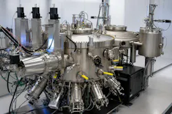
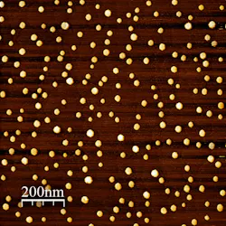
The growth of QDLs requires precise control of substrate temperature, III-V fluxes, and epitaxial interfaces, which can be best achieved by molecular-beam epitaxy (MBE). Reflection high-energy electron diffraction (RHEED) adds real-time, in situ monitoring of surface morphology and quantum dot formation to support tighter control of the self-assembly process.
Recent MBE developments by Veeco target tighter flux uniformity, more accurate temperature management, and greater process automation. Our production MBE platforms incorporate SUMO effusion cell and nozzle technology to deliver highly uniform flux that varies less than 1% across the platen with optimized material utilization.
Developed through close partnership between Veeco and k-Space Associates, integrated in situ metrology measures the actual substrate surface temperature during growth rather than relying only on indirect temperature indicators. Real-time temperature feedback enables closed-loop heater control and tuning to achieve substrate temperature non-uniformity less than 5°C across the platen, while also improving run-to-run absolute substrate temperature consistency.
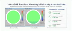
The value of tighter flux and temperature control is ultimately measured in the benchmark device structures. For distributed Bragg reflector (DBR) structures near 940 nm and 1300 nm, the combined process improvements limit wafer-to-wafer wavelength differences to less than 3 nm, with a wavelength standard deviation below 0.063% within wafer. This level of control supports the wavelength reproducibility and manufacturing yield required for QDLs and other advanced photonic devices.
Looking ahead, Veeco is advancing the integration of additional in situ metrologies for real-time flux monitoring, film-strain characterization, and Smart RHEED analytics to enable smarter MBE systems. Our dedicated MBE applications lab is working on MBE platforms that support new products, as well as customer process development. This level of quantum dot growth expertise is vital for an MBE partner to support customers in process development, optimization, troubleshooting, and manufacturing scaleup.
An ‘and’ future
One of the most common misconceptions surrounding QDLs is they will replace InP technology. The reality is AI infrastructure growth is occurring at such a rapid pace that multiple laser technologies will likely be required to satisfy future demand. InP EMLs will continue serving large segments of optical networking and datacom applications, while QDLs may emerge as complementary solutions for applications where power efficiency, thermal resilience, integration density, or system architecture requirements favor their unique attributes. Ultimately, QDL adoption is expected to be gradual and complementary rather than disruptive.
For equipment suppliers, chip manufacturers and systems companies alike, the question is no longer whether optical interconnects will expand throughout AI infrastructure. The question is: Which technologies will enable the next phase of this expansion?
The answer includes both today’s proven InP solutions and tomorrow’s quantum-dot-enabled architectures. By supporting innovation across metal-organic chemical vapor deposition (MOCVD) and MBE ecosystems and partnering with photonics leaders developing next-generation devices, Veeco is helping position the industry for sustained growth as silicon photonics transitions from a promising technology to a foundational pillar of the AI era.
About the Author
Matt Gossen
Matt Gossen is the senior product marketing manager, MBE, for Veeco Instruments Inc.
Stephen Farrell
Stephen Farrell is director of applications at Veeco Instruments Inc.
Xi Dong
Xi Dong is a research scientist for Veeco Instruments Inc.