Are high-power laser diodes ready to power inertial fusion energy?
After more than 60 years and tens of billions of dollars in public funding for fusion research, during the past five years we saw a shift toward private investment. Inertial fusion energy (IFE) alone received more than $1.5B in private funding during the past two years, which demonstrates the commercial potential of IFE as a carbon‑free, safe, and scalable energy source.
This shift is largely being driven by the National Ignition Facility’s (NIF) fundamental achievement of net target gain in December 2022, and multiple subsequent confirmations that the physics of IFE is no longer the limiting factor. The emphasis has now moved to engineering the necessary hardware: Materials, targets, and, most importantly, semiconductor laser diodes. An ecosystem of technology advancements, manufacturing excellence, and a skilled workforce is needed to support this emerging need. Southern Arizona can take a leading role through its growing semiconductor industry, the presence of key laser diode manufacturers like Leonardo Electronics US Inc., and the education of a skilled workforce by local institutions.
Laser diodes are a critical component
Laser diodes are widely regarded as the critical component that can make IFE commercially viable. A future IFE power plant will consist of many thousands of laser diode modules. It’s evident that the size, among functional parameters, is of utmost importance because it drives the power plant footprint.
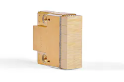
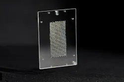
Compact laser diode arrays (LDAs) are achieved by maximizing the light-emitting area over the passive (dark) area—fitting the maximum laser bars into a stack and maintaining this high brightness when multiple stacks are combined into modules. Leonardo Electronics US’s T6 heatsink can routinely hold more than 50 bars and has been shipped in high volume for decades. It enables 2D stacking with minimal addition of passive area and micro-optics that manipulate the complex beamlets into an output beam of useful dimension and homogenized intensity distribution. Manufacturing the necessary micro-optics can be a lengthy, tedious, and expensive process, but Leonardo developed a fast, accurate, and inexpensive approach.
While state-of-the-art bars now routinely achieve and exceed 1 kW of output, increasing this power without also increasing the semiconductor area could further increase brightness and reduce cost. A double-junction architecture provides twice the peak power at the same current and a nearly identical form factor, but it also doubles the heat load and requires better thermal solutions and more work on reliability, efficiency, and optical collimation. These bars represent the most direct path to higher brightness and lower cost per watt, and they will play a central role in the next generation of diode modules.
Efficiency at the stack level is equally critical. Recent data demonstrates that modern stacks can achieve wall‑plug efficiencies near 60% at the kilowatt-per-bar operating point. High stack-level efficiency not only reduces waste heat and cooling system requirements but also lowers the operating temperature and extends diode lifetime. The reduction in voltage and current decreases the demand on the electrical drive system. As a result, the overall efficiency gain of a fusion power plant is more than just the incremental gain in diode efficiency.
Focus on reliability and cost
While reliability remains a central challenge for IFE-class laser diodes, in the short term it’s not a roadblock to IFE deployment progress. Systems such as high-repetition rate advanced petawatt systems (HAPLS), after 10 years of operation, demonstrate meaningful laser system utilization, because current use conditions rarely demand ON-times at full pulse repetition rate or 24/7 operation. In the long term, however, requirements are becoming more demanding.
At Photonics West 2026, Lawrence Livermore National Laboratory presented reliability targets on the order of 5 Gigashots—a level that requires improvements in efficiency, heat extraction, and facet protection. The Starfire collaborative, with participants from Germany, France, the U.S., and Japan, aims to establish a global reliability testing standard to accelerate qualification cycles and unify expectations across the IFE supply chain.
Cost remains the largest barrier to economical diode use for fusion, and solving it is fundamentally a manufacturing challenge. Reaching a price point below $10/kW won’t happen through volume alone—it requires a purpose‑built manufacturing ecosystem that combines deliberate engineering, high automation, robust supply chains, and sustained investment. The III–V edge‑emitting laser industry today resembles the silicon industry decades ago: High manual labor content, limited automation, non-standardized processes, high variability, and extensive in‑process testing.
Arizona’s emerging semiconductor hub offers an opportunity to establish a new manufacturing model informed by lessons from the silicon industry. With T6 architecture as a building block, state‑of‑the‑art peak power, and micro‑optics that enable module miniaturization without brightness loss, Leonardo is well positioned to translate these manufacturing advances into low‑cost, high‑performance diode modules produced in Arizona.
Building a resilient manufacturing environment where the design, manufacture, and test of high‑performance diodes can thrive requires a capable workforce supply, and Arizona is developing this infrastructure. Supported by the Arizona Board of Regents, the University of Arizona has declared IFE a major thrust and, in collaboration with private companies such as Leonardo, serves as an education and research institution. Local partners like Pima Community College, the Southern Arizona Center for Optics and Photonics, and Optics Valley are investing in technician and operator training to create a workforce pipeline tailored to advanced diode production. Together, these institutions position Tucson and Southern Arizona as the place where low‑cost, fusion‑grade laser diodes can be manufactured at scale and anchor a global IFE supply chain.
As inertial fusion energy moves from scientific breakthrough to commercial reality, scalable and cost-effective laser hardware is the key to moving from laboratory demonstrations to viable power plants. Our high-power diode architectures, including high‑brightness T6 modules, advanced micro‑optics, double‑junction bars, and manufacturable processes, provide the foundation for fusion plant designs. With regional support from the University of Arizona and the broader semiconductor ecosystem within Arizona, we can create a place where cutting-edge diode technology, skilled workforce development, and a robust manufacturing base converge. This combination positions Southern Arizona not just as participants, but as essential enablers of delivering the compact, efficient, reliable, low-cost megawatt-class modules at scale that are critical to making fusion a practical source of clean energy for the world.
ACKNOWLEDGEMENT
The author thanks Leonardo’s Laurel Lunsford, Patrick Keiffer, and Prabhu Thiagarajan for their valuable contributions and assistance in completing this article.
About the Author
 Lukas Gruber
Lukas Gruber
Lukas Gruber is Leonardo Electronics’ business development director.