‘Nanoridge’ surface-emitting lasers grown directly on 300-mm silicon wafers
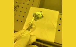
A Belgian collaboration between the groups of Professor Dries Van Thourhout, who leads the photonics research group at Ghent University, and Bernardette Kunert, a scientific director at imec and pioneer of nanoridge arrays, led to the creation of nanoridge surface-emitting lasers (NRSELs) grown directly on 300-mm silicon wafers (see Fig. 1 and video).
Several years ago, Professor Susumu Noda from Kyoto University (now also an honorary professor at Ghent University) presented a way to overcome the limitations of traditional vertical-cavity surface-emitting lasers (VCSELs) during a CLEO Europe conference. It inspired Van Thourhout, who was exploring novel approaches to create electrically injected lasers monolithically integrated on a silicon substrate.
Later, when Van Thourhout looked at scanning electron microscope (SEM) images of nanoridges Kunert sent to him, he realized the extremely regular arrays of nanoridges should, in principle, act as a photonic crystal cavity capable of forming a laser cavity.
Nanoridge epitaxy backstory
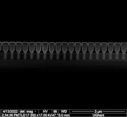
The group’s gallium arsenide (GaAs) NRSEL concept is based on Kunert’s pioneering nanoridge engineering work at imec, which is a monolithic III-V integration method (see Fig. 2).
To demonstrate the first application of nanoridge engineering, Kunert and her epitaxy group worked with Joris Van Campenhout and his optical input/output R&D team at imec and initially focused on a III-V Fabry-Perot laser device with a nanoridge as a waveguide (its etched facets form the laser cavity) to enable edge emission. “It resulted in the first III-V laser devices fully fabricated on 300-mm silicon substrates within the complementary metal-oxide semiconductor (CMOS) prototyping line at imec,” Kunert says.
Kunert previously worked with VCSEL devices, so she’s familiar with the intricacies involved in growing VCSEL devices and found it “intriguing to shift to NRSELs, which require significantly less III-V material.”
While the desire for direct III-V devices grown on silicon substrates has long existed, dating back to research during the 1980s, “the principal obstacle remains attainment of high crystal quality within the III-V film deposited on silicon,” Kunert explains. “Nanoridge engineering addresses this challenge by using selective area growth inside narrow trenches. Notably, the total nanoridge growth duration on patterned 300-mm silicon substrates is only 1 to 2 hours.”
Achieving precise III-V growth to form a desired structure “is demanding, largely because the nanoridge presents a 3D geometry that features multiple crystal facets for epitaxial deposition,” Kunert says.
Engineering nanoridges “requires a deep understanding of the fundamental growth behaviors that occur on different crystal surfaces,” Kunert points out. “We also discovered that the quality of trench patterning, purity of the silicon/silicon dioxide wafers, and pre-treatment of wafers prior to growth are all very critical factors to create uniform nanoridge arrays.”
NRSEL design work
To create NRSELs, Van Thourhout’s group uses Kunert’s nanoridges with embedded indium gallium arsenide (InGaAs) quantum wells to provide gain that forms a second-order grating (see Fig. 3). “When the period and other dimensions are well chosen, such an array forms an efficient laser cavity,” says Van Thourhout. “The optical mode resonates in plane, and part of the light escapes vertically to form a nice beam that’s useful for many practical applications.”
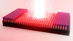
As far as materials, “the breakthrough is that the gain material—GaAs/InGaAs—is grown directly on 300-mm silicon substrates by Kunert and it’s compatible with large-scale fabrication,” Van Thourhout explains. “This is possible, thanks to aspect ratio trapping and nanoridge engineering techniques invented by imec, which suppress all defects due to lattice mismatch within a small region. Material grown on top of it is very high quality.”
Before beginning their experiments, Eslam M.B. Fahmy, a Ph.D. student and main researcher involved in this project, ran simulations (mostly FDTD) to explore the viability of their idea and design. “We could immediately verify several ideas for further improvement, such as bottom and side mirrors for higher Q and better light confinement,” says Van Thourhout.
After Fahmy received wafers from Kunert with uniformly grown nanoridge III-V material on standard 300-mm silicon, he did the cleanroom fabrication work to define the laser cavities and implement the mirror and cavity structures needed for surface-emitting lasing. It’s important to note that “because nanoridges are only a few hundred nanometers tall, their growth takes significantly less time than the thick distributed Bragg reflector mirror stacks used for conventional VCSELs,” he says.
The overall process “is sophisticated because it combines III-V epitaxy with 300-mm silicon processing,” Fahmy adds. “One of the key advantages of this platform is that it reduces complexity compared to traditional VCSEL-type approaches, because the lasing condition comes from a photonic crystal cavity rather than from thick DBR mirror stacks.”
‘Immediately certain it was lasing’
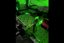
The coolest part of the work for Fahmy was “seeing the devices light up brightly above threshold for the first time,” he says. “I’d spent so much time on the simulations, the device physics, and the cavity design that seeing all of it finally come together in a structure that actually emits bright laser light was an amazing moment. I was so excited I left the lab and rushed to bring Professor Van Thourhout back with me so he could see it too.”
When Fahmy showed Van Thourhout how the cavities lit up superbright on the camera—going from completely dark to very bright with just the slightest variation in pump power—they were “immediately certain it was lasing, but it took us another two years to gather enough data to be able to prove it in a scientific paper,” says Van Thourhout.
For Fahmy, seeing a mechanism like a bound state in the continuum—which can sound almost purely theoretical—doing real work within a practical device was thrilling. “It confines light inside nanoridges only about 500-nm tall above a silicon substrate, but also enables vertical surface emission from a very small footprint,” he says.
Nanoridges act as much more than simply the gain medium—they also form the photonic crystal cavity and optical confinement, and allow the light to couple out vertically. “This is what makes the platform so elegant and powerful,” says Fahmy.
Wafer-scale manufacturing and co-integration ahead
Since the devices are epitaxially grown on standard 300-mm silicon wafers, “the approach aligns naturally with wafer-scale manufacturing and with co-integration alongside electronics and silicon photonics,” says Fahmy. “While our work demonstrates optical pumping, electrical injection isn’t far away (see Fig. 4). It will require more engineering—especially for contact design, so that current can be injected without disturbing the optical mode or blocking the surface emission.”
It looks feasible because “we electrically pumped edge-emitting nanoridge lasers a few years ago,” says Van Thourhout. “But the actual demonstration will require considerable development.”
VCSELs are “one of the most commonly used types of lasers, found in optical interconnects and consumer products such as optical mice and face recognition for phones,” Van Thourhout adds. “In principle, our NRSEL devices should be able to address all of these types of applications—using a less costly fabrication process (in volume).”
FURTHER READING
E.M.B. Fahmy et al., Light Sci. Appl., 15, 120 (2026); https://doi.org/10.1038/s41377-025-02061-z.
About the Author

Sally Cole Johnson
Editor in Chief
Sally Cole Johnson is Laser Focus World’s editor in chief, and she has more than 25 years’ experience as a science and technology journalist. She specializes in physics and semiconductors, and wrote for the American Institute of Physics for more than 15 years, and also covered theoretical physics and neuroscience for the Kavli Foundation, and complexity for the Santa Fe Institute. Johnson has also written extensively about military embedded systems, high-performance computing, software-defined networks, and infosec. She is a member of the National Association of Science Writers (since 2001).
When she isn’t writing about optics, photonics, or quantum advances, you can find her outside in northern NH in the garden with birds landing in her hand or heading for the mountains with her bike, skis, or crampons and ice axe.