Nanolaser opens door to new class of photonic devices
A nanolaser created by Technical University of Denmark (DTU) researchers led by Jesper Mørk, a professor of quantum and laser photonics, moves us a step closer to on-chip data being transmitted entirely via photons (see video). Thousands of these nanolasers can potentially be placed onto a single microchip, which could not only help speed up devices and data centers but reduce their energy consumption by as much as 50%.
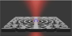
The group’s research focuses on nanocavities that confine light to ultrasmall length scales.
“For many years, it was widely believed within the photonics world that plasmonic cavities—cavities incorporating metals—are required to localize light to dimensions far below the optical wavelength,” explains Mørk. “But we’ve shown that similar confinement can be achieved by using purely dielectric materials, such as III-V semiconductors.”
This discovery opens the door to a new class of photonic devices with enhanced functionality and reduced losses. “One of our main research directions is nanolasers,” Mørk says. “We refer to this broader research as ‘extreme dielectric confinement,’ which reflects our ambition to push light confinement in dielectric materials to unprecedented scales.”
III-V semiconductor materials
The group’s nanolaser is based on III-V semiconductor materials, with an active region formed by an indium phosphide (InP)-based quantum well. The optical cavity geometry isn’t derived from conventional intuition but rather topology optimization—an advanced computational design method that systematically searches for structures that maximize desired optical properties. This work was done in collaboration with Professor Ole Sigmund at DTU.
“A substantial part of our project involved developing nanofabrication processes required to create these highly complex cavity geometries with sufficient precision,” says Mørk. “In particular, surface passivation was essential to suppress nonradiative recombination and maintain high material quality at the nanoscale.” The nanofabrication work was led by Professors Kresten Yvind and Elizaveta Semenova from DTU Electro.
How does the group’s nanolaser work? Electrons within the quantum well are excited using an optical pump laser to create material gain within the nanocavity. Lasing occurs when the rate of stimulated emission exceeds the total optical losses of the cavity.
Because the cavity “strongly confines light to an extremely small volume, the interaction between the optical field and the electronic gain medium is significantly enhanced,” says Mørk. “This enables lasing at very low pump powers.”
As far as simulations work, Mørk’s DTU colleague Yi Yu developed a comprehensive mathematical model of the nanolaser that accounts for both the spatial distribution of excited carriers and the optical field profile inside the cavity. “Understanding the spatial overlap between the confined optical mode and the excited electrons is crucial for efficient laser operation, and the simulations were instrumental in explaining the measurements done by Meng Xiong and for identifying mechanisms governing performance,” says Mørk.
Electrically pumped versions ahead
For practical applications, electrical pumping is essential. “A few years ago, we demonstrated a different type of nanolaser that achieved the lowest threshold current ever reported for a room-temperature laser—below one microampere.1 Commercial semiconductor lasers typically operate at threshold currents roughly a thousand times higher,” says Mørk. To the best of their knowledge, this record still stands.
“Our goal is to leverage the technology developed for that device to create electrically pumped versions of our nanolaser. The most significant challenge is achieving deterministic localization of injected carriers in the optical hotspot of the cavity,” Mørk says. “We’re addressing this issue through several approaches because controlled carrier localization is also critical for other nanophotonic devices, including single-photon sources for quantum information technologies.”
On-chip optical interconnects
One key application area for the nanolaser is on-chip optical interconnects. “Today, electrical interconnects are used, for example, between processor cores. But resistive (ohmic) losses lead to significant energy dissipation and heat generation, which must be actively managed,” says Mørk.
Optical interconnects may dramatically reduce energy consumption and heat generation, but the semiconductor lasers currently used for fiber-optic communications are too large and consume too much power for dense on-chip integration. “So demand is growing for ultrasmall, ultra-efficient lasers that operate at very low energy per bit—precisely the niche targeted by nanolasers,” Mørk says.
What’s next for Mørk’s group? “The next major milestone is the demonstration of electrically driven nanolasers with high quantum efficiency,” he says. “Achieving this requires a deeper understanding and precise control of light-matter interactions within nanostructures, as well as advances in nanoscale fabrication techniques.”
This field presents fascinating fundamental and technological research challenges, which makes it particularly suited for university research. “If the necessary foundational work proceeds successfully, practical electrically pumped nanolasers based on our concept could emerge within the next five to 10 years,” Mørk says.
FURTHER READING
M. Xiong et al., Sci. Adv., 11, 51 (Dec. 17, 2025); https://doi.org/10.1126/sciadv.adx3865.
REFERENCE
1. E. Dimopoulos et al., Optica, 10, 8, 973–976 (2023); https://doi.org/10.1364/optica.488604.
About the Author

Sally Cole Johnson
Editor in Chief
Sally Cole Johnson is Laser Focus World’s editor in chief, and she has more than 25 years’ experience as a science and technology journalist. She specializes in physics and semiconductors, and wrote for the American Institute of Physics for more than 15 years, and also covered theoretical physics and neuroscience for the Kavli Foundation, and complexity for the Santa Fe Institute. Johnson has also written extensively about military embedded systems, high-performance computing, software-defined networks, and infosec. She is a member of the National Association of Science Writers (since 2001).
When she isn’t writing about optics, photonics, or quantum advances, you can find her outside in northern NH in the garden with birds landing in her hand or heading for the mountains with her bike, skis, or crampons and ice axe.