Tunable diode lasers: A path to practical quantum systems
The second quantum revolution, Quantum 2.0, is driven by advances in generating and manipulating quantum states in both light and matter, which enable new applications such as quantum sensing, computing, and communications. These applications leverage unique quantum properties— superposition, entanglement, and enhanced measurement sensitivity—to offer fundamental advantages over classical technologies. At the foundation of these capabilities are Quantum 1.0 technologies, particularly single-frequency lasers, often followed by stabilization hardware and downstream optics and optoelectronics that condition the light for a range of operations required by each quantum platform.
To date, most quantum implementations have relied on discrete, lab-grade lasers and associated light conditioning components. Among laser sources, tunable diode lasers emerge as the most widely used, thanks to their advantages over gas and solid-state lasers in terms of cost, size, and efficiency.
Diode laser architectures for quantum applications
A range of diode laser architectures were developed to meet the stringent linewidth and frequency-stability requirements of quantum applications, including external-cavity diode lasers (ECDLs), distributed feedback (DFB) lasers, and distributed Bragg reflector (DBR) lasers. These laser platforms can be combined with semiconductor-tapered amplifiers or fiber amplifiers to achieve higher output powers, and with nonlinear optical frequency conversion processes such as harmonic generation, optical parametric oscillation (OPO), and sum- and difference-frequency generation to access wavelengths from the deep-ultraviolet (UV) to the mid-infrared (IR) not directly available from laser diodes.
Beyond the lasers themselves, the hardware used for frequency stabilization and light conditioning, including active modulation and passive beam shaping and routing, is largely based on bulk optics and adjustable optomechanics.
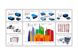
Macro-optic laser systems
A representative set of “macro-optic” laser systems (see Fig. 1) manufactured by TOPTICA Photonics spans multiple architectures, including ECDL-, DFB-, and DBR-based sources, semiconductor and fiber amplifiers, and frequency-converted lasers, further complemented by adjacent technologies such as ultrastable clock lasers and difference-frequency combs. These systems cover all quantum-relevant wavelengths from 200 nm to 4 μm and provide high beam quality, single-frequency operation with linewidths ranging from sub-hertz to megahertz, and low phase and relative intensity noise (RIN). The company also manufactures T-RACK systems to provide rack-based modularity for complex, multiwavelength configurations, which enable the integration of multiple lasers, difference-frequency combs and extensions, wavemeters, and laser control and locking electronics.
Quantum information science is advancing from laboratory research toward technology demonstrations, and the need to transition from discrete lasers and optical components to integrated laser engine systems is becoming increasingly clear. Such a transition is driven by requirements for scalability, autonomous operation, ruggedness, and reduced size, weight, and power (SWaP) to enable field deployability.
While macro-optic-based lasers and light-conditioning hardware offer flexibility for alignment and system configuration, their component-level architectures, with relatively relaxed constraints on size and ruggedness, limit scalability and deployment outside controlled laboratory environments. This challenge is particularly evident in fault-tolerant quantum computing, which requires the creation, manipulation, control, and readout of quantum states across large numbers of physical qubits.
Meeting these demands necessitates a dramatic increase in the density, stability, and robustness of optical control signals. But conventional lab-grade lasers, optics, and optoelectronics lack the scalability and cost structure required to support this level of hardware integration. The requirements become even more stringent for practical quantum sensing, metrology, and quantum communications. These applications often demand low-SWaP hardware with ruggedized designs, autonomous operation, extended uptime in field environments, and the potential for high-volume, cost-effective manufacturing.
Application-specific micro-integrated laser engines
One promising near- to mid-term approach to addressing these challenges is the development of application-specific micro-integrated laser engines, which are attracting interest especially within the quantum sensing community. Such systems leverage advances in the development, assembly, and packaging of micro-optic-based lasers and downstream active and passive components. TOPTICA eagleyard’s miniECLs (volume Bragg grating-stabilized ECDLs) and miniPAs (semiconductor amplifiers) are an example of advances within this realm.1,2 Their hermetically sealed construction and low-SWaP designs make these devices well suited for micro-integrated laser engines, especially for field-deployable quantum sensing applications.
While micro-optics may offer the most straightforward path toward practical quantum systems in the near- to mid-term, they continue to face challenges in achieving cost-effective, batch-scale fabrication and in integrating diverse components into complex, highly functional systems within a truly low-SWaP form factor. In contrast, optimal quantum hardware is increasingly envisioned to be built on technologies that support dense miniaturization and integration of a broad range of active and passive photonic components alongside embedded microelectronic and radio frequency (RF) elements. Within this context, photonic integrated circuits (PICs) and optoelectronic integration are emerging as promising enablers for such advanced quantum systems. PICs would equip quantum systems with new capabilities such as improved performance and integrability, reduced SWaP and cost (SWaP-C), and scalable fabrication through batch processing, thereby accelerating the transition of quantum technologies to the marketplace.
Quantum-relevant PICs
Quantum-relevant PICs and associated microelectronics and RF integrated circuits are far less mature than those used in other technologies such as telecom or datacom. Quantum technologies use a variety of wavelengths—often at the visible and UV ranges—and require different materials and solutions that must be tailored to the individual wavelengths. The main challenge with using multiple wavelengths is the need for miniaturized and stabilized lasers at all relevant wavelengths, and each one often requires its own gain material development and optimization effort.
Other elements of the PICs will also need design and optimization for each wavelength. Fabrication recipes for low-loss waveguides, modulators, couplers, splitters, filters, isolators, etc. can be highly wavelength-dependent, which makes it particularly challenging to engineer PICs that simultaneously support multiple wavelengths. This “rainbow problem” could prove to be the quantum PIC industry’s greatest challenge.3
Quantum PIC integration and packaging challenges
Beyond the challenges associated with the maturity of quantum PIC platforms, the integration and packaging of these systems pose significant obstacles. Quantum systems are inherently multidisciplinary, and the integration of quantum PIC platforms—whether hybrid, heterogeneous, or monolithic—remains highly underdeveloped.
Modular PIC architectures may require multiple interconnects, but the technology for fabricating these interconnects, including fiber-to-chip, chip-to-chip, and chip-to-free-space connections, involves complex and costly alignment procedures and remains a work in progress.
Ruggedization is another critical requirement for field-deployable PIC quantum systems, which must be fully assessed and verified. For this technology to scale and transition from the lab to practical applications, it needs to withstand field conditions such as temperature and pressure fluctuations, space radiation, and other extremes, while performing reliably for extended periods without maintenance or technical service.
And the quantum market itself presents a significant hurdle. Unlike the more established markets for technologies enabled by lasers and enhanced by PICs, such as telecom and datacom, the quantum market remains small and fragmented, but rapidly evolving. This makes investments in advancing quantum PIC technologies challenging, because prototyping, testing, and scaling PIC-based quantum systems is too costly for many organizations.
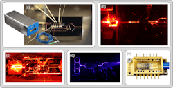
Despite this, many photonic developers are exploring quantum-relevant PIC components and systems. TOPTICA Photonics is pursuing several inhouse and collaborative projects to develop various architectures of PIC-based tunable diode lasers at different wavelengths for a range of quantum applications (see Fig. 2).
Collaboration is key to advance quantum PICs
What will it take to advance quantum PICs? A synergistic approach, due to the challenges and multifaceted complexity of quantum systems that can’t be addressed through fragmented R&D efforts. This approach needs a combination of public and private investments and partnerships to accelerate the development and adoption of PIC technologies for the emerging quantum market. To achieve this, long-term partnerships between universities, national laboratories, and industry are essential to take the innovation process from research to development to commercial deployment.
Sustainable investments, particularly by governments, will be crucial in creating or enhancing low-volume foundry capabilities and leveraging existing nascent commercial competencies. Government-supported resources such as the Microelectronics Commons Hubs in the U.S. and the Quantum Flagship programs in the European Union can accelerate the development of these markets by serving as early adopters of PIC-based quantum technologies for government missions. Accelerating the development and adoption of these technologies will enable the emerging quantum market to realize its full potential and transition from laboratory settings to practical, scalable operations.
REFERENCES
1. D. Brauda et al., Proc. SPIE, 12402, 1240204 (2023).
2. H. Thiem et al., CLEO/Europe 2023 and EQEC 2023, cb_p_11 (2023).
3. M. A. Tran et al., Nature, 610, 54–60 (2022).
4. M. C. Zanarella et al. Optica Open preprint (2026); https://doi.org/10.1364/opticaopen.31013068.v1.
5. J. Nojic et al., CLEO/Europe 2025 and EQEC 2025, cb_p_11 (2025).
6. L. V. Winkler et al., Opt. Express, 32, 17, 29710–29720 (2024).
7. C. A. A. Franken et al., Nat. Commun., 16, 10294 (2025).
8. L. V. Winkler et al., IEEE Photonics J., 15, 5, 1-8 (2023).
About the Author
Siamak Dadras
Siamak Dadras is a senior quantum application scientist at TOPTICA Photonics (Pittsford, NY).