Laser cooling GPU chips at the nanophotonic level?
It’s no secret data centers struggle to contend with heat generation and power consumption issues. Sandia National Laboratories and University of New Mexico (UNM) researchers recently joined Maxwell Labs, a startup based in Minnesota, on a quest to explore laser-based photonic cooling as a new way to regulate the temperature of high-density processors and lower power consumption, while also increasing the efficiency of today’s data center air- and water-based cooling systems (see video).
Using lasers for cooling isn’t an entirely new concept, but using them to chill systems at the nanophotonic level is. It will be a truly huge technology disruption—imagine chips not overheating—if the team succeeds.
For this quest, Maxwell Labs is handling the design work, Sandia researchers are building the devices, and then UNM researchers will analyze the thermal performance of the devices.
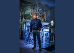
“Sandia is involved with this project because bulk cooling doesn’t appear to be feasible,” says Sandia Physicist Raktim Sarma. “We’re targeting very localized hot spots—on the order of hundreds of microns—because it may turn into a new way to cool chips.”
Sarma has spent the past few years making photonic hardware for low-power, high-speed data processing. He also works on inverse design, which is a computer design optimization technique where you use a figure of merit and design your photonic structure to achieve it. The idea is simple: An inverse design photonics structure targets the laser light when it enters the tiny hotspot, then chills it.
“When I first heard about Maxwell Labs’ work from their CTO and cofounder Alejandro Rodriguez (as well as a professor of electrical and computer engineering at Princeton University), whom I’d worked with in the past on inverse design, I realized this work brings together my two areas of interest,” Sarma says. “The goal is to use inverse design to make photonic cold plates to address this heat/power-consumption issue of data processing within AI data centers. It’s different but also synergistic with the work I’ve been doing making photonic hardware for low-power high-speed data processing, so I was intrigued.”
Laser cooling concept
Rodriguez is a physicist by training, so his brain naturally gravitates toward addressing the fundamental sources of engineering challenges. “Thinking about not only current but future power density problems in data centers, and the hard and prohibitive limits of conventional cooling technologies, it became clear to me that what’s truly needed is a re-imagining of the way heat management systems address the multiple spatial and temporal scales present within modern microprocessors,” he says.
Light is “not only a fast carrier of energy and information but can also be localized and controlled down to atomic scales, which enables us to exploit quantum physics that fundamentally alters the way heat is carried in and out of materials—effects that lie beyond the realm of classical convective and conductive cooling techniques,” Rodriguez explains. “The ability to control refrigeration down to micron and picosecond scales and to reach temperatures far below ambient by simply dialing the laser power of a source external to a chip offers fundamentally new ways of extracting heat. This vastly unexplored nature of this frontier inspired us to dig deeper.”
The concept of laser cooling was largely pioneered by the late UNM Professor Mansoor Sheik-Bahae and his lab. Lasers can cool when a specific light frequency is paired with a very pure target of specific materials. For example, lasers can help hold individual atoms at supercold temperatures for quantum computers.
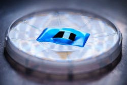
Unlike existing cooling systems today that work by flowing cold water through microscopic channels within copper cold plates atop a chip to absorb heat, the light-based cold plate designed by Maxwell Labs channels cooling laser light to the hotspots. These photonic cold plates may replace or assist water- or air-based cooling systems to enable heat extracted in the form of light to be recycled and converted back into electricity.
Targeting and controlling localized heating spatially and at optical timescales can “unlock thermal design constraints so fundamental to chip design that it’s difficult to speculate what chip architects will do with it,” says Maxwell’s CEO Jacob Balma.
Materials and design challenges
There’s no shortages of materials and design challenges ahead for the team. Laser cooling is a very inefficient process—on the order of 1 or 2%. And shining laser light heats up material impurities—the undesirable opposite of cooling—so a photonic cold plate needs to be designed with extremely pure epitaxial layers of crystalline GaAs to work.
While demonstrations at the lab level have already been done at UNM to cool very thin GaAs, the team’s photonic cold plates will need to be thicker. “This is a challenge because a thicker material isn’t ideal—it gives us both materials and design challenges,” Sarma says. “Our goal is to inverse design the photonics structures to overcome these challenges.”
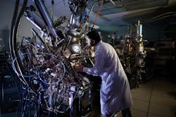
And this is where Sandia Materials Scientist Sadhvikas Addamane’s expertise with molecular beam epitaxy (MBE) and growing wafers comes in.
The MBE process involves “ultrahigh-purity sources, which allow us to precisely control the material’s thickness,” explains Addamane. “We grow these epitaxial layers under ultrahigh vacuum.”
Beyond the purity challenge, the researchers also face bandgap issues. “The defect and dislocation levels we can tolerate are lower than normal for other III-V semiconductor materials. As we progress, we’ll need to optimize and change our design,” Addamane adds. “There’s a certain limit of how pure we can make it—we’ll hit a dead end. And once we reach it, we’ll need to redesign our structure and illumination methods, architecture, etc., to be able to still cool it with the purity levels we get. We don’t know exactly what these numbers are yet, but we’ll find out once we build this system up.”
High-power lasers aren’t necessary for the Sandia researchers to test whether the devices are working or not on their end. “We’ll use a broadband light source to check that the photonic structure has the optical response we want,” Sarma says.
But the next step is thermoguide positioning, a.k.a. real-time temperature monitoring, and it’s where UNM uses high-power lasers to analyze the thermal performance of the devices. After Sarma and Addamane create these photonic cold plate structures and attach them to rare earth ion crystals, UNM researchers will do a cooling demonstration via high-power lasers that operate around 1-µm wavelength.
Timeline
So far, the researchers have demonstrated the different components and used inverse design for nonlinear optics applications—a light-matter couple system. “Addamane has tons of experience growing high-quality GaAs epitaxial structures,” points out Sarma. “And UNM has been working on laser cooling for decades. We have all of the different components, now we need to combine them.”
The team’s initial cooperative research and development agreement (CRADA) is for two years. “We’re hoping to have a proof of concept that the idea works at a single chip level within a year to 18 months,” Sarma adds. “It won’t be the final product, but our goal is to show we can cool things at the microscopic level using these structures.”
Some of the “most impactful technological developments of the past century have come from application of fundamental physics that at the time seemed unrelated, exotic, or useless in relation to the technological problem at hand,” says Rodriguez. “The very development and application of the laser as a generator of information—which now rules over so much of our daily lives—comes to mind. I believe we’re standing at the precipice of one such major disruption here: Light is often thought of as a source of heat, not a remover of it. This counterintuitive aspect of optics makes laser cooling one of the coolest aspects of our work, pun intended.”
FURTHER READING
S. Stich et al., ACS Nano, 19, 18, 17374–17384 (2025); https://doi.org/10.1021/acsnano.4c16934.
About the Author
Sally Cole Johnson
Editor in Chief
Sally Cole Johnson, Laser Focus World’s editor in chief, is a science and technology journalist who specializes in physics and semiconductors.


