Electrically controlled quantum dots unlock new possibilities
Quantum dots are nanoscale semiconductor structures with unique properties that have long been heralded for their potential in various applications. They can also be used to trap excitons, which are bound electron-hole pairs formed when a material absorbs photons. A new approach to achieving electrical control of optically active quantum dots overcomes traditional limits on scalability and precision—enhancing prospects for the use of excitons and quantum dots in future cutting-edge applications such as photonic quantum computing.
Interest in excitons relates to their inherent qualities. Unlike photons, these short-lived quasi-particles have electric charges, which makes them an attractive interface between electronics and photonics. In the few picoseconds before re-emerging as luminescence, excitons can be manipulated in distinctive ways, for instance, through the application of electrical fields.
A team of scientists from NTT Research, the Swiss Federal Institute of Technology (ETH) Zürich, and Stanford University, co-led by me and ETH Professor Puneet Murthy, introduced a method not only for confining excitons electrically, but also for measuring and scaling them up through arrays of quantum dots and other geometries.
Results and experimental setup
We demonstrated that you can decide where to trap the exciton, but also at which energy it will get trapped. Electrical control matters for scalability. This technique maintains a well-defined voltage potential across a tiny junction in a manner not architecturally different from complementary metal-oxide semiconductor (CMOS) technologies that control gate voltages on billions of transistors.
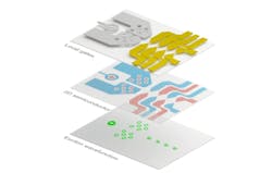
The controlled interactions in these experiments occurred on heterostructure devices comprised of a 2D semiconductor flake—0.7 nm or three atoms thick—in the middle, sandwiched between a global bottom-gate electrode and a top-gate layer where nanoholes and bow ties were etched to define excitonic confinement (see Fig. 1). To avoid thermal fluctuations, these devices were cooled to 5 Kelvin (-450°F) within a closed-cycle dry cryostat with optical access.
The most important advantage of our approach for electrical nanoscale control of excitons is the potential for scaling up to more complex structures. Our quantum dot and other trapping methods can be viewed as the building blocks for larger systems. An important motivation was to achieve multiple quantum dots with identical energies, which is a crucial ingredient for applications like photonic quantum information processing and quantum communications.
Maintaining identical energy levels has been a hurdle, because existing material modulation approaches are drastically limited by material disorder and process variation. Cost plays a role, too. One way to bring two confined excitons to the same level, for instance, is to replicate an experiment. In other words, two samples in two different setups. That approach, however, is hardly conducive to scaling, given laboratory equipment costs.
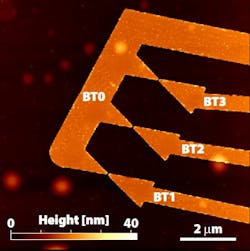
We address the problem by fabricating an array of bow ties with independent control for each. Figure 2 shows three bow ties with gap size of 50 nm and a separation of 1 μm. We electrically short the left-hand side electrodes of the three (BT0), while maintaining individual control on each of the right-hand side electrodes (BT1, BT2, BT3). This allows us to reduce the number of control gates per quantum dot to one, which enhances scalability without compromising on control.
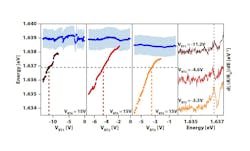
Our team reports the fitted energy of the quantum dot states as a function of individual gate voltages (VBT1, VBT2, and VBT3), while keeping the common counter electrode (VBT0) constant (see Fig. 3). The 2D exciton’s energy is shown with blue dots. Three bow ties show different dependence with voltage, possibly due to material disorder and variations due to nanoscale fabrication uncertainties. But the three dots can be simultaneously tuned to degeneracy by applying the suitable voltages across the bow ties. This is evident in the spectra shown in Fig. 3, which shows three quantum dot states resonantly tuned in energy.
Basic physics and applications
The ability to combine position-controlled, lithographically defined quantum dots with simultaneous and independent energy tunability into scalable arrays of quantum sites is a major result of our approach. A key advantage is that it can be extended to any 2D semiconductor, and improvements in fabrication techniques will enable even smaller trapping length scales and better spatial control.
Optical computation, one potential application, requires interactions between photons, which is analogous to what occurs when transistors block electrons or allow them to flow. The question we addressed is: How far we can push this in optics? What is the minimum number of photons that we need to control other photons?
Our results revealed several new directions not only for possible future applications, but also for fundamental physics. This versatile technique can define quantum dots electrically, which provides an unprecedented level of control over the properties of the semiconductor at the nanoscale. The next step is to investigate deeper the nature of light emitted from these structures and find ways to integrate them into cutting-edge photonics architectures.
FURTHER READING
J. Hu et al., Sci. Adv., 10, 12 (Mar. 20, 2024); https://doi.org/10.1126/sciadv.adk6369.
About the Author
Thibault Chervy
Thibault Chervy is group leader and senior research scientist of the PHI Lab at NTT Research.