Purely silicon light emitter for silicon photonics is CMOS compatible
It is very hard to produce a usable amount of light from silicon using electricity. This is a big problem for silicon photonics, because a complete optical integrated circuit on silicon needs a light source. Currently, hybrid light sources using III-V semiconductor emitters are a candidate, but they require complicated bonding or growth processes to unite them with the silicon circuit. There is also research going on with germanium-silicon (Si-Ge), which, if mechanically strained, can be made to emit light.
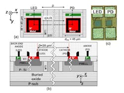
Now, Satadal Dutta, a researcher at the University of Twente (Enschede, Netherlands), says that he has developed a silicon-based light source; this light source, the corresponding photodetector, and the waveguides to connect them can all be made using the CMOS technology that is used to make electronic circuits.
What is particularly attractive about Dutta's approach is that no special materials or manufacturing processes are needed: the light comes only from silicon.
Avalanche LED emitter
Silicon only emits a tiny amount of infrared light; in addition, a detector made out of silicon requires visible or very near-IR light. The two devices are talking and listening at different wavelengths. Dutta's solution was to connect a CMOS-compatible silicon LED in reverse; at low voltages, there's no current or light, but at a high-enough voltage, there arises a small current that amplifies itself. In this "avalanche mode," the LED produces visible light. Using the same CMOS process, the photodetector, as well as the connecting waveguide and passive components, can be fabricated.
Uses
An optical link on a chip is a good way to electrically isolate two circuits from each other. This is often necessary in cases where one circuit is a low-voltage and low-current one, while the other is a high-power circuit. They should be connected, but not by conducting wires, for reasons of safety. A classic transformer is always an option, but an optical connection is often used instead. Until now, this has been a separate optocoupler, which is large and has limited speed.
Dutta's new device is much more compact: in total, it is just a few tens of microns in size, and yet still offers the protection needed at higher bit rates. Compared to optical channels in full optical circuits, the energy consumption of the device is relatively high, as there is some scattering of light. On the other hand, designing electronics around the optical link can be an efficient way to keep the amount of light needed for a successful connection to a minimum.
Source: https://www.utwente.nl/en/news/!/2017/11/287829/electronics-and-optics-on-one-chip
About the Author
John Wallace
Senior Technical Editor (1998-2022)
John Wallace was with Laser Focus World for nearly 25 years, retiring in late June 2022. He obtained a bachelor's degree in mechanical engineering and physics at Rutgers University and a master's in optical engineering at the University of Rochester. Before becoming an editor, John worked as an engineer at RCA, Exxon, Eastman Kodak, and GCA Corporation.

