PHOTONIC FRONTIERS: Nanopatterns impose order on quantum-dot lasers

Progress in diode lasers has been shaped largely by a series of improvements in confinement of current carriers and photons. The ultimate step might seem to be lasers with active layers that include quantum dots, which confine electrons on a nanometer scale in three dimensions. But no sooner have quantum-dot lasers reached the market than developers are working on an interesting new twist, arranging quantum dots into regularly spaced nanopatterns that impose more order on the dots in the laser's active layer.
Today's quantum-dot lasers are fabricated by a self-assembly process that fills the active layer with dots of a range of sizes and shapes that are not regularly spaced. Despite that seeming disorder, self-assembled quantum-dot lasers have advantages over conventional quantum-well lasers. These include lower thresholds, higher efficiency, and less temperature sensitivity. Some quantum-dot researchers are now exploring the potential for further performance improvement by arranging the quantum dots into neatly ordered structures in the active layer.
Basics of quantum wells and dots
Like quantum wells, quantum dots trap electrons in potential wells where their energy is lower than in the surrounding material. The big differences are dimensional. A quantum well is a low-energy planar layer sandwiched between two layers with higher electron energy; in contrast, a quantum dot is a nanometer-scale three-dimensional volume with low potential energy surrounded on all sides by a higher-potential material.
Typical quantum dots are 2 to 50 nm across, and contain hundreds to millions of atoms. A single free electron trapped in such a small volume can occupy a number of discrete energy levels analogous to those of an outer-shell electron in an atom. This capability gives quantum dots properties similar to those of single atoms, leading to conceptually simple systems. The exact energy levels, and the transitions possible, depend on the size of the dot, as well as the composition.
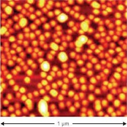
First made in the 1980s, quantum dots were successfully incorporated into diode lasers in 1994, and room-temperature operation was demonstrated in 1996. The standard approaches to fabricating quantum-dot active layers are based on molecular-beam epitaxy (MBE) or metal-organic chemical vapor deposition (MOCVD). A low-bandgap quantum-dot material such as indium gallium arsenide (InGaAs) is deposited on a higher-bandgap barrier layer such as gallium arsenide (GaAs). Spots of InGaAs initially start growing at random locations on the GaAs surface, but once InGaAs islands form, the indium compound preferentially grows on the indium-rich material. The larger the chemical mismatch, the higher the quantum dot grows up from the surface. The dots thus self-arrange themselves on the active layer (see Fig. 1). Then they are coated with a barrier layer of a higher-bandgap material such as GaAs.
The science of quantum-dot lasers is now well understood, says Pallab Battacharya of the University of Michigan (Ann Arbor, MI), who edited a special issue of the Proceedings of IEEE on quantum-dot optoelectronics in September 2007.1 But it took time to develop that understanding. A decade elapsed from the time he and two other groups demonstrated the first room-temperature quantum-dot lasers until the company now known as Innolume (Dortmund, Germany) introduced a commercial broadband quantum-dot laser in 2006. "Full realization of the theoretical advantages has required years of molecular-beam epitaxy process development, heterostructure engineering, and device optimization," according to Innolume's Web site. QD Laser (Tokyo, Japan) announced a quantum-dot laser last year, and this year launched a 10 Gbit/s version optimized for telecommunications.
The small size of quantum dots makes them less sensitive to strain than larger semiconductor structures, relaxing the normal lattice-matching constraints in III-V compounds and increasing the range of wavelengths available. The self-assembly process also increases the emission bandwidth because it forms quantum dots at a range of sizes, giving a spread of energy levels and emission bands. Innolume has reported emission bandwidths of tens of nanometers for its quantum-dot lasers. The gain is relatively even across that range—a big plus because it enhances performance of semiconductor optical amplifiers. Quantum-dot lasers also have very low threshold current, as well as better temperature stability and lower chirp than quantum-well lasers.
Spatial and spectral control
Despite these successes, some developers want to push the frontier further. Although self-assembly packs quantum dots together efficiently, the process has an inherently random nature in terms of how it arranges quantum dots in size and space. Could fabricating arrays of quantum dots or similar structures that are uniform in size and distribution improve performance?
James Coleman of the University of Illinois (Urbana-Champaign, IL) thinks such control might make new devices useful for applications such as advanced photonic signal processing. "The inability of self-assembly techniques to provide sufficient spatial and spectral control of quantum dots for advanced applications has driven development of more explicit techniques for fabrication," he and Victor Elarde wrote in a review paper.2
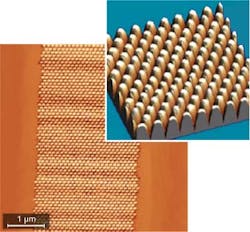
They have explored photolithographic fabrication of regular arrays of quantum dots. Photolithography couldn't fabricate nanometer-scale structures when quantum dots were first developed, but it can now produce structures down to tens of nanometers. Conventional photolithography used for electronic chip production can't yet reach the dimensions of the smallest quantum dots, but feature sizes continue to shrink, and some advanced techniques can reach smaller sizes.Interference of deep-ultraviolet light can be combined with photolithography to produce very closely spaced grids with regular spacing to form nanopatterns quickly over large areas (see Fig. 2). However, it is inherently limited to producing uniform and regularly spaced features. Electron-beam lithography can produce arbitrary features down to tens of nanometers, but it takes much more time because the beam must sequentially scan the entire surface. It can be combined with selective-area epitaxy to produce a very uniform array, or to make patterns including quantum dots of two different sizes, says Elarde, now at QPC Lasers (Sylmar, CA).
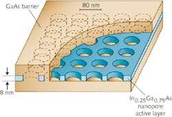
To demonstrate feasibility of the technique, Elarde and Coleman made ridge-waveguide and buried-heterostructure lasers with patterned arrays of InGaAs quantum dots in their active layers (see Fig. 3).A buried-heterostructure design had a threshold current density of only 280 A/cm2. That didn't match the 159 A/cm2 threshold of a quantum-well device they made as a control, but Elarde says, "We weren't really expecting to get better thresholds than quantum wells." He explains that threshold can always be optimized by adjusting the design; their goal was to demonstrate their process worked.2 The important result was that the spectral data showed quantum size effects and matched theoretical predictions, validating the model.
Nanopore active layers
Elarde and Coleman also devised a "nanopore" array they call "the inverse of a patterned quantum-dot active layer," because it swaps the positions of the high-bandgap barrier layer and the low-bandgap core of the quantum dot. They start by etching a regularly spaced array of nanopores into an InGaAs quantum-well layer deposited on a higher-bandgap GaAs barrier, then fill the holes with GaAs and cover the quantum-well layer with the same barrier material.
The quantum-well layer remaining between the nanopores has an energy-level structure that resembles that of quantum dots surrounded by barrier layers, but with some important differences. The remaining areas of the quantum well retain physical connections, so they couple to each other more strongly than the separate quantum dots. That process forms energy bands that are distributed through the structure, and creates a higher-state density. This density promises higher gain than is possible with quantum dots, but complex calculations are needed to determine the energy states.
The properties of the nanopore structure depend on the size and spacing of the pores, the thickness of the active layer, and the composition of the quantum-well layer and the barrier. Changing the configuration can vary properties widely. "If the pores all touch, in the space between, you have a star-shaped region, not a round dot, but it's still a quantum bit of stuff," says Coleman. "If the pores get really sparse they have no impact, and [the structure] looks like a quantum well."
Research on the nanopore structure is still in an early stage, but a theoretical analysis matches experimental observations of spectral emission.3
Outlook
Self-assembled quantum-dot lasers have reached the market, and Battacharya expects them to carve out niches where their performance benefits are important. Further tweaking of processes and performance can improve the technology, but he says that's engineering rather than fundamental science.
Nanopatterning of quantum dots is fundamentally a new adventure, and like all such explorations of the unknown, it has potential but can't guarantee results. Coleman hopes his work on quantum dots will lead to advanced photonic devices, but says his real interest is in fundamental things like atoms. "If you make things little enough to be quantized, but big enough not to be individual atoms, you get the best of both worlds."
REFERENCES
1. Proc. IEEE 95 Special issue on Optoelectronic Devices Based on Quantum Dots, Battacharya et al., eds. (September 2007).
2. V. C. Elarde and J. J. Coleman, Prog. Quantum Elect. 31, p.225 (2007).
3. V. Boehm Verma et al, IEEE J. Quantum Electronics 45, p. 10 (January 2009).
About the Author
Jeff Hecht
Contributing Editor
Jeff Hecht is a regular contributing editor to Laser Focus World and has been covering the laser industry for 35 years. A prolific book author, Jeff's published works include “Understanding Fiber Optics,” “Understanding Lasers,” “The Laser Guidebook,” and “Beam Weapons: The Next Arms Race.” He also has written books on the histories of lasers and fiber optics, including “City of Light: The Story of Fiber Optics,” and “Beam: The Race to Make the Laser.” Find out more at jeffhecht.com.


