PHOTONIC FRONTIERS: EUV LITHOGRAPHY: EUV lithography has yet to find its way into the fab

Extreme ultraviolet (EUV) sources are the future of semiconductor photolithography—and they have been in the future for long time. Those with a long view could see the trend of shrinking chip features in the 1990s, as 248 nm krypton-fluoride (KrF) laser sources replaced mercury lamps, and 193 nm argon-fluoride (ArF) lasers were developed for even smaller geometries. By 2003, EUV sources had found a place about a decade out on the semiconductor development roadmap.1 Now it's 2013, and EUV has yet to reach the factory floor.
"The EUV source has turned out to be much more challenging than we had thought," says Stefan Wurm, director of lithography at Sematech (Albany, NY). Timetables slipped. Double-patterning with 193 nm immersion systems is producing chips with 32 nm features, and higher levels of multiple patterning are coming online for the next generation. But the pace of EUV development accelerated in 2011, Wurm says, when ASML (Veldhoven, the Netherlands), which builds complete lithography systems, "stepped in and took more ownership of the source," investing more resources in EUV and agreeing to buy Cymer (San Diego, CA), a major source manufacturer.
That decision is now paying off. At the SPIE Advanced Lithography meeting2 (Feb. 24–28, 2013) in San Jose, Cymer reported a new EUV source that delivered average powers of 40–55 W at 13.5 nm for long periods and is offering a new generation of sources based on that technology. The output power has yet to reach the levels needed for commercial chip production, but Wurm called the demonstration "a very significant milestone." He says the next major milestone will be delivery of the new-generation sources in coming months. Yet others, such as lithography consultant Chris Mack (Austin, TX), worry that EUV lithography may be too late to succeed.
Lithography sources and requirements
Photolithography has been crucial to decades of progress in electronics. A light source exposes a photoresist coated on the chip surface, the exposed areas are removed, and the surface is etched to define features. Then the process is repeated for additional layers to build up an integrated circuit. The feature size depends on the source wavelength, focusing optics, and the photoresist.
Moore's Law scaling of chip features to smaller sizes has driven the march to shorter wavelengths, with today's production systems based on the 193 nm ArF laser. Developers settled on the big step to 13.5 nm in the late 1990s, picking the wavelength to match the peak reflectivity of the best available EUV mirrors—multilayer structures of silicon and molybdenum. Although laser and high-harmonic sources can reach that band, tin plasmas were picked because they are simpler and brighter at 13.5 nm.
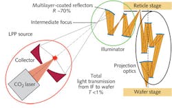
Lithography sources are packaged in a lithography machine or system, which includes optics that illuminate a pattern mask or reticle with light from the source, and focus the reflected light onto a photoresist-coated wafer, as shown schematically in Fig. 1. The systems are large, complex, and very expensive, and the economics require a source that delivers enough light to expose about 100 wafers/hr. The sources are pulsed, and exposure is cumulative over many source pulses.
EUV sources
The EUV-emitting tin plasmas are produced by zapping molten tin droplets with pulses from a carbon-dioxide (CO2) laser or from an electric discharge. Cymer and Gigaphoton (Oyama-shi, Tochigi-ken, Japan) use lasers; Xtreme Technologies (Aachen, Germany) uses discharge excitation directed by a laser beam.
Cymer has already produced 10 copies of its developmental model 3100 EUV source, a Q-switched CO2 master oscillator/power amplifier (MOPA) with three amplifier stages that operates at repetition rates of 40 to 50 kHz. Each pulse hits a single tin droplet. Average power of the laser is 15 kW, which was enough to deliver an average EUV power of 11 W to the photoresist and expose up to 7 wafers/hr at customer sites last year. Five of the sources are being used in process development at chip manufacturers, three are used at Cymer, and two are at ASML.
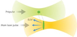
Cymer achieved the 40–55 W EUV power reported at the SPIE meeting by adding a fourth amplifier stage to the CO2 laser and by illuminating tin droplets with a prepulse before the main pulse, says Nigel Farrar, vice president of technical marketing. He says that power was sustained in long bursts over long periods and under realistic operating conditions. The prepulse technology improved results by expanding the 30 μm tin droplet to 100 μm, matching the size of the focused beam so it would absorb more energy from the main pulse, as shown in Fig. 2.Refinements in the forthcoming 3300 source, including increasing the size of the collecting mirror, should raise the delivered EUV power to 70–75 W, Farrar adds. Cymer's roadmap includes two higher-power sources, a 125 W version pumped by a 31 kW CO2 laser and a 250 W version pumped by a 43 kW laser.
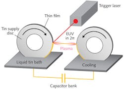
At SPIE, Gigaphoton reported that its developmental EUV had delivered average EUV output of 10 W and a peak of 20 W EUV output when tin targets were hit by a solid-state laser prepulse before more powerful CO2 pulses at 100 kHz.3 Xtreme uses a laser pulse to trigger an electric discharge between two wheels coated with liquid tin, as shown in Fig. 3.Optics and other issues
Working in the EUV poses some important complications in optics and power delivery. As shown in Fig. 2, the tin plasma radiates in all directions, and the collection mirror can direct only part of that light toward that lithography system. Transparent optics are not usable in the EUV, so lithography sources must use multilayer mirrors. "[EUV] optics are reasonably mature," says Farrar, with mirror reflectivity close to the theoretical maximum of 70% for normal incidence. However, losses are higher for the ellipsoidal collector, which also must be kept clean of splattered tin.
Losses add up because complex optics are needed for illuminating the mask with light from the EUV source, and projecting an image of the mask onto the resist. The system shown in Fig. 2 uses 10 mirrors, so if each reflects 70% of the input light, only 2.8% of the original power remains—and that does not count losses in the collector, reflection loss from the mask, and light not absorbed by the resist. Those losses are a prime reason that average EUV power delivered to the wafers remains short of the levels needed to produce the 100 or more wafers per hour needed to pay for the costly systems.
Moving to the EUV raises other problems. Photon energy is more than 10 times higher than at 193 nm, so new resists are needed, and electrons released by the energetic photons can spread in the material. As chip geometry shrinks, defects become an increasing problem. "We don't have the capability of even detecting the defects on the mask that we think are going to harm us," says Mack. He expects line roughness to become a major problem at feature sizes of 10 nm.
Alternative lithographic technologies
The main competition to EUV lithography is coming from multiple-patterned 193 nm lithography. "At SPIE there were reports of quadruple or octuple patterning," says Wurm. Big companies are keeping their options open, looking at extending 193 nm technology and exploring EUV as they move to smaller feature sizes.
Another contender is directed self-assembly, which uses 193 nm sources to create templates that guide small building blocks to assemble themselves into semiconductor structures. "We have seen dramatic progress in the last couple of years," Mack says. "It's a way to multiply the capabilities of 193 nm immersion lithography." Wurm thinks the concept "is going to take a long time" to implement but may be attractive as a complement to lithography.
However, directed self-assembly does not compete against EUV sources. "It is a replacement for conventional photoresist," not a piece of equipment, says Dan Herr of the University of North Carolina (Greensboro, NC). It could be adapted to use EUV sources as well as 193 nm sources to provide the top-down control for self-assembling structures that grow from the bottom up.
Looking forward
It all adds up to a complex picture, further complicated by the fact that different parts of the semiconductor industry have different needs. "The ones most eager for [EUV] technology are the foundries," says Wurm. They don't control the design of the chips they make, so single-exposure EUV fabrication is much more attractive than multiple exposures at 193 nm.
Extreme ultraviolet will be introduced selectively for layers and structures hard to fabricate with multiple exposure lithography, predicts Wurm. "The layers where EUV will be used first are contact hole layers," he says, which have to be very small and clean. Other layers on the same wafers could be printed with multiple patterning. With many issues to be resolved, the transition may be slow.
The real milestone now, says Wurm, is that the technology "has moved from the hands of the researchers into the hands of the engineers." The engineers will use the new tools to develop the new processes and test how well they can produce the next generation of chips. Their job is not easy, but it's a very important one.
REFERENCES
1. International Technology Roadmap for Semiconductors, 2003 edition; http://bit.ly/13m5fIq.
2. 2013 SPIE Advanced Lithography Program; http://bit.ly/ZYtduQ.
3. G. Overton, "EUV light source from Gigaphoton reaches 20 Watt output," Laser Focus World online (Feb. 20, 2013); http://bit.ly/16fKsbz.
About the Author
Jeff Hecht
Contributing Editor
Jeff Hecht is a regular contributing editor to Laser Focus World and has been covering the laser industry for 35 years. A prolific book author, Jeff's published works include “Understanding Fiber Optics,” “Understanding Lasers,” “The Laser Guidebook,” and “Beam Weapons: The Next Arms Race.” He also has written books on the histories of lasers and fiber optics, including “City of Light: The Story of Fiber Optics,” and “Beam: The Race to Make the Laser.” Find out more at jeffhecht.com.


