Bonder design meets telecom challenges
DON MOORE
Packaging optoelectronic components for the telecommunications industry is getting more complicated as vertical-cavity surface-emitting lasers (VCSELs) move from R&D into mainstream use in fiberoptic communication. This is particularly true for original equipment manufacturers (OEMs) and contract electronics manufacturers (CEMs) that are either transitioning into the telecom arena from other markets or trying to keep pace with the telecommunication industry's increasingly varied laser use.
Presentation/pickup challenges
Initial challenges for companies new to the market include attaching diode lasers to submounts within the required minimum ±5-µm placement precision, along with simply handling the delicate tiny devices during the bonding process. In semiautomatic bonding operations, which is what most of the new companies start out with, diode lasers arrive at the bonding station in either waffle packs or Gel Paks, although some firms prefer to use a mirror-like tray because the mirror aids in aligning the bonder's pickup tool with the target die on the tray. The carrier containing the die is manually placed on a die tray pedestal, which is usually sized to hold two or four carriers containing all die or a combination of die and gold/tin preforms. If the die carrier is a Gel Pak, the pickup head on the bonder must not be too hot because the gel in the carrier is heat sensitive.
When working with VCSELs, a "precising" station on the bonder's pickup pedestal serves two purposes. It enables the VCSEL to be taken from the Gel Pak with an unheated tool without damaging the Gel Pak prior to handling with a preheated tool for placement on the submount. It also holds the VCSEL firmly in place so that when the pickup tool lands on the VCSEL its emission point is not moved off center from its alignment with the bonding system's overlay image.
The bond head on the pickup tool must be either flat-faced with vacuum or a two-sided collet because the crystal facets on the opposite ends of edge-emitting diodes must not be touched by the bonder's pickup tool. Touching can create flaws that cause faulty operation or even complete failure of the diode.
Since gold/tin alloy is the predominant bonding material used to attach diode lasers for the telecom industry, the pickup tool needs to be equipped with a dual head—one for the die and one for the gold/tin preform. Although not specified yet for telecom use, epoxy bonding of VCSELs, particularly in computer communications applications, is gaining favor with some packagers. For those applications, the bonding system design must include a special epoxy transfer tool for depositing precise amounts of epoxy.
Alignment/placement challenges
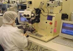
By far, the most challenging aspect of bonding diode lasers is achieving the accuracies that are required in aligning and placing the die on the submount's bond site (see Fig. 1). However, certain applications, particularly those involving the placement of VCSELs on the top of round transistor outline (TO) headers require more alignment/ placement capability than is achievable using just a cube beamsplitter and scope. The problems encountered for this type of application are virtually insurmountable without the use of special viewing features on the laser bonder.
To begin with, the operator cannot see the VCSEL's emission point after the VCSEL has been picked up out of its carrier because the pickup tool holding the die blocks the view. While the laser's emission point usually is placed on the center of the TO header, it frequently is located off center on the diode laser because of the need to make room on the laser chip for the bonding pad.
Therefore, during placement of the VCSEL on the submount, the emission point needs to be aligned to a specific feature on the submount. In some cases, the feature is a fiducial mark. In aligning the emission point to the center of the header, the issue is further complicated by the fact that the TO header is a machine-stamped piece of metal, for which tolerances may vary. For instance, if the TO header shoulder is out of round by a certain amount, it can adversely affect placement accuracy if not detected and corrected for.
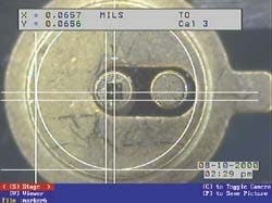
In expensive and sophisticated automatic bonders, the pattern recognition system looks at the chip while it is sitting in the carrier and memorizes where the emission point is. But adding such capability to a semiautomatic bonder is not a viable option. Engineers at Semiconductor Equipment Corporation, therefore, use a relatively inexpensive but effective video image marker. It has enabled relative newcomers on the telecom scene such as Teledyne OptoElectronics (Marina Del Rey, CA) to achieve the desired ±5-µm placement precision of the emission point on any TO header. It also can be used for aligning to other types of submount surfaces.The video image marker consists of a keyboard, a control box and X-Y knobs for adjusting the system's magnified electronic images. The video image marker creates and stores a fixed video overlay of cross hairs in the form of a bit map for centering the VCSEL's emission point, as well as up to 10 different video patterns that can be superimposed on the submount on which the VCSEL is to be bonded. An example of the latter would be a circle overlay image of the outside diameter of the top of a TO header (see Fig. 2). Custom patterns also can be created.
ACKNOWLEDGMENTS
The author would like to thank Teledyne OptoElectronics (Marina Del Rey, CA) and, in particular, Robert Clarke, director of process engineering, for assistance in the preparation of this article.
Don Moore is president of Semiconductor Equipment Corp., P.O. Box 8079, Moorpark, CA 93020; e-mail: [email protected].

