In the early years of their history, diode lasers seemed miraculous for their small size. By the time the quantum well was developed, researchers had realized that device structures could be made even smaller. These reductions in size have provided unexpected benefits in device performance and reliability.
The active layer of a quantum well is on the order of 10 nm, roughly 40 atomic layers (a four-atom-wide layer is about one nanometer thick). The electrons and holes of the layer at this level of confinement are trapped on a two-dimensional sheet of material where quantum effects dominate their behavior.
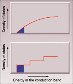
At classical dimensions, the number of energy states in the conduction band available to an electron making a jump from the valence band increases gradually with increasing energy. Only the states closest to the conduction-band edge, however, contribute to electron-hole recombination (the electrons fall back to the valence band) and so produce photons. Electrons at higher levels must first lose energy before contributing their laser photons.
One step at a time
This “density of states” in the conduction band has a different distribution for a quantum well. The available states now take on a stair-step distribution, so that more electrons can jump to a given energy range, and more states are available in the vicinity of the conduction-band edge (see Fig. 1). This results in higher efficiency and faster response, as the laser reaches threshold more rapidly.
When quantum wells are combined with strained layer technology, a reduction in temperature sensitivity is an additional benefit. Recall that a strained layer accommodates a mismatch in the crystal lattices of alloys used in adjoining layers. The thin quantum-well layer can accommodate about a 1% mismatch in lattice constant. The resulting strain in the lattice impedes the propagation of nonradiative electron-hole recombination, which produces heat instead of light.
Nonradiative recombination takes place in the lattice of the active layer, the valence band. The sensitivity of the laser to such processes is described by a parameter called the characteristic temperature—Ith. The higher the Ith is, the slower the corresponding rise in threshold current with temperature will be. Strained-layer quantum-well designs can double the characteristic temperature for some alloys used in the gain region.
Confining the charge carriers in the active layer in width as well as thickness places an even higher density of states within a given range of energies, lowering the threshold current for lasing still further. Such one-dimensional structures are called “quantum wires.” Difficulties in developing such structures come from keeping uniform widths of only a few tens of atomic layers for the length of the laser cavity.
Zero dimensional lasers
By trapping the charge carriers to quantum size confinement in three dimensions—a “quantum dot”—researchers may achieve the ultimate in laser speed and efficiency. To produce a vertical-cavity surface-emitting laser (VCSEL) with an array of quantum dots in the gain regions, molecular-beam epitaxy is used to deposit a layer of the active material only a few atoms thick on a buffer layer. When the buffer-material crystal is in a certain orientation and under the correct temperature conditions, the thin active material “beads up” on the buffer crystal just as water beads up on a glass surface. Layers of such quantum-dot arrays can be stacked to form the entire gain region of a laser.
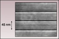
Engineering lasers one atomic layer at a time has been put to use in a different context. By combining hundreds of alternating layers each a few atoms thick, it is possible to divide the energy gap, rather than the density of states, into a step-like arrangement (see Fig. 2). Infrared output can thus be achieved from semiconductors that normally produce visible light. Such quantum cascade (QC) lasers using gallium arsenide (GaAs), for example, are made with a wide range of micron-length wavelengths.Something completely different
For almost 40 years, so-called “lead-salt” devices have been the diode lasers of choice in this wavelength region. These are mostly in spectroscopy, most commonly the detection of gaseous compounds. All together these applications, such as pollution detection, comprise a billion-dollar-a-year market served primarily by nondiode light sources.
Lead-salt lasers rely on the familiar relationship of bandgap to photon energy to produce outputs from roughly 3 to 30 mm. (The “salt” in the name refers loosely to the type of crystalline structure of the alloys.) They are made from semiconductors with bandgaps less than 0.5 eV—most commonly from alloys of lead and tin from group IV, and tellurium, selenium, and sulfur from group VI, with europium often used as a dopant.
As is typical of other devices at these wavelengths, lead-salt lasers rely on cryogenic cooling to avoid being overwhelmed by room-temperature black body radiation. The longer-wavelength lasers are sometimes even cooled by liquid helium. The upside of this sensitivity to temperature is that it is used for wavelength tuning, important for the complexities of molecular spectra. Fine-tuning is accomplished by small changes to drive current, which in turn change the temperature of the active layer.
Spectroscopists measure wavelength in an energy term called wavenumber, the inverse of the wavelength as measured in centimeters. The tuning range of lead-salt diode lasers in the mid-IR is about 50 cm-1. The actual picture is complicated by the longitudinal-mode structure of the laser. The gain curve of the lead-salt alloys is broad enough to span the mode structure of the 250 mm or so cavity length typical of the devices, but nevertheless they tend to operate in single longitudinal-mode.
The tuning range within a single mode is about 1 cm-1 or perhaps somewhat more before the output hops discontinuously to the next mode. Equally important to tuning is linewidth and stability—single modes are less than 0.001 cm-1 wide, and have a long-term stability of about this same value.
Still worth their salt?
Lead-salt lasers do suffer considerable handicaps compared to other diode laser types. They are low-power devices, on the order of a milliwatt, with the output tapering off for longer-wavelength lasers. Lead-salt performance at longer wavelengths has always been problematic. (To avoid diffractive losses, the gain region of the device must be made excessively thick). In each of these areas, the new quantum cascade lasers have a marked advantage.
Originally proposed by Kazarinov and Suris of the Soviet Union in 1971, QC lasers were finally realized in 1994 at Bell Labs (Holmdel, NJ). A QC laser consists of hundreds of alternating layers, each a few atomic layers thick. It is this layer thickness, rather than the intrinsic material property of the semiconductors, which determines the energy of the emitted photons. Varying the layer thickness while still using the exact same semiconductor alloy can change the laser wavelength (see Fig. 3).A waterfall of electrons
Quantum cascade lasers have been described as an electronic waterfall, but really the term “cascade” in the name is most descriptive. A single electron injected at the edge of a cascade layer emits a photon as it falls to the lower energy state of that particular band. Then, owing to the extreme thinness of the layer, it “tunnels” through to the higher energy state of the next cascade layer, where it again emits a photon with an energy determined by the layer thickness. The whole process may be repeated 50 times for a single electron.
Compared to lead-salt lasers, the cascade design makes these devices intrinsically high-power and environmentally robust. Perhaps most significantly, they are capable of pulsed operation at room temperature, and deliver an order of magnitude more CW power than lead-salt lasers when they are cooled. Their increased power and room-temperature operation should lead to their use in some existing applications, such as breathalyzers and LIDAR, and perhaps enable new applications altogether, such as collision-avoidance systems for automobiles.
Borrowing for improvements
By combining the basic QC principle with other diode laser structures, developers have been able to improve and extend QC laser performance. The incorporation of a distributed feedback grating as a reflector has produced a wider tuning range without the same type of discontinuities found in lead-salt lasers. Incorporating a so-called "superlattice" structure, QC lasers that simultaneously emit multiple wavelengths have been developed.
Quantum-cascade laser operation in the far-IR has proven difficult, as absorption loss at the longer wavelengths reduced stimulated emission below lasing level. By using a behavior of light in a crystalline structure known as a surface plasmon, Bell Labs researchers recently were able to concentrate the light at the metallization interface in a waveguide effect. The result is a 20-mm output and a cryogenically cooled peak-power of 15 mW.
Some important molecular species are not yet covered by reported QC laser wavelengths—notably CO2. There appears to be an impediment to developing QC lasers tailored to meet infrared applications, however. An interesting question is whether or not quantum cascade technology can be extended to different material systems—perhaps as a means of obtaining other wavelengths not currently produced by diode lasers.
Next month the series concludes with a look at next-generation developments in diode-laser research.REFERENCE
- J. Faist et al., Appl. Phys. Lett. 68, 3680 (1996).
About the Author
Stephen J. Matthews
Contributing Editor
Stephen J. Matthews was a Contributing Editor for Laser Focus World.

![FIGURE 2. The ability to fabricate structures only a few atomic layers thick allows the creation of lasers with output controlled entirely by device dimensions, rather than material properties. The diagram is a representation of a Quantum Cascade laser, comprising hundreds of GaAs layers to emit at infrared wavelengths [1]. FIGURE 2. The ability to fabricate structures only a few atomic layers thick allows the creation of lasers with output controlled entirely by device dimensions, rather than material properties. The diagram is a representation of a Quantum Cascade laser, comprising hundreds of GaAs layers to emit at infrared wavelengths [1].](https://img.laserfocusworld.com/files/base/ebm/lfw/image/2016/01/th_0201feat8_2.png?auto=format,compress&fit=max&q=45?w=250&width=250)
