Lasers tool up for via formation
David Moser
WITHIN THE PAST FIVE YEARS, THE USE OF INDUSTRIAL LASERS TO FORM SMALL LAYER-TO-LAYER ELECTRICAL PATHS (VIAS) IN PRINTED CIRCUIT BOARDS HAS MATURED FROM AN EXPERIMENT TO A STANDARD PRODUCTION PROCESSMiniaturization and performance improvements are driving the electronics industry to shrink the size of semiconductor packages and greatly increase the density of printed circuit boards. This is enabling new opportunities for the use of solid-state ultraviolet (UV) lasers in volume production of these components. There are several emerging market opportunities for laser systems including micro-via formation, electronic circuit tuning (laser trimming), and micromachining of electronic components. This article will focus on the micro-via application, which is currently experiencing rapid growth, and on the emerging UV laser opportunity. Within the past five years, the use of industrial lasers to form small layer-to-layer electrical paths (vias) in printed circuit boards has matured from an experiment to a standard production process. This has enabled a new generation of handheld electronic equipment such as ultra-small cell phones, high performance palm computers, and advanced technology digital cameras. In addition, new semiconductor packaging designs are using micro-vias for the new chip scale packages and high-performance ball grid array packages.
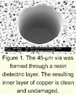
The most common micro-vias today are blind vias, which connect the outer layer of a circuit to the underlying inner layer. Figure 1 shows a blind via, which was formed by a diode-pumped UV laser. Other designs require multilevel vias or vias completely through all of the layers, which can be fabricated in many constructions and a wide variety of dielectric materials. This wide range of applications has led to the development of several new laser processes, including CO2 laser for larger vias (75 to 150 µm), excimer lasers for some packaging designs, and diode- pumped ultraviolet Nd:YAG lasers for vias down to 25 µm in diameter.
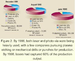
The production of circuit boards with micro-vias started approximately in 1995, with IBM's facility in Yasu, Japan, using a photo-imageable dielectric for via formation. The electronics industry refers to micro-via production as High Density Interconnect (HDI) in North America and Europe, and Build Up Multilayer (BUM) in Asia and Japan. Figure 2 shows the production growth rates and the technology trends. By 1996, both laser and photo-via were being heavily used, with a few companies pursuing plasma etching or mechanical drills or punches for production. By 1998, lasers had captured 60% of the production output. By 1999 the production volumes were significantly higher and lasers had captured 70% of the market.
The total micro-via production is expected to continue growing exponentially over the next several years. The requirement for micro-via circuits has recently been extended to include most of the semiconductor packages for the worldwide microprocessor market, and will soon include the main circuit boards for PCs and servers. There is also a significant acceleration to the technology shift being provided by cost and productivity improvements. Recent estimates indicate that HDI technology will become the lowest-cost process for most multilayer circuit board applications.
Ultraviolet laser technology opportunities
As the micro-via market continues to mature, there are laser technology improvements that would greatly improve the acceptance of UV laser technology and expand the total available market. The main benefits of the diode-pumped Nd:YAG or YLF UV lasers in production today are:
- High UV absorption in all of the materials used in the industry, including organic resins, copper, and glass. This provides the ability to ablate all of these materials for via formation.
- Small focused spot size, which enables via production to 25 µm diameter or smaller. In some applications, the 4th harmonic of YAG (266 nm) can form vias with extremely high aspect ratios. In one product, 35-µm vias are formed through substrates over 425 µm thick.
- Lower thermal damage to the organic dielectric material than infrared processes such as CO2 laser. UV laser vias also require less cleaning and demonstrate less substrate delamination.
- Selective ablation of materials by varying the fluence level of the UV energy on the work surface. This enables blind vias through an outer layer of copper that do not damage the inner copper layers.
These advantages have enabled UV lasers to become the dominant technology for vias <75 µm. However, to maximize the future potential of this technology, the rate of UV laser improvement must accelerate. There are several primary areas requiring improvement. The first is to increase laser power by providing the current pulse energy at higher pulse repetition rates. Researchers also are working to provide consistent laser beam quality including maintaining proper beam shape, eliminating satellite beams, controlling the pointing stability, and providing identical beam characteristics over many lasers. Other issues include improving pulse-to-pulse stability over a wide range of laser duty cycles and pulse repetition rates and increasing long-term laser and optics life expectancy for industrial environments, where the operating year is over 8500 hr.
These improvements will provide the required performance for the next generations of high-density circuit boards and semiconductor packages. The overall market for diode-pumped, solid-state UV lasers will steadily rise as more of the worldwide production shifts to this technology.
David Moser is Marketing Manager of Advanced Packaging Products for Electro Scientific Industries, Inc., Portland, VA. He can be contacted by (P) 503/671-5549 or e-mail: [email protected].
Reprinted from Industrial Laser Solutions, May 2000.


