Beam-shaping optics expand excimer-laser applications
ANDREW MASTERS and THORSTEN GEUKING
Most applications for excimer lasers require the output beam to be modified by homogenizing and then reshaping the beam profile to match the application. Novel optics and optomechanical design are used to transform the beams.
Excimer lasers are used in an increasingly diverse range of industrial and scientific applications because of their unique ability to deliver high pulse energies and high average power at UV wavelengths. However, the rectangular beam produced by most excimer lasers must usually be reshaped to match the needs of the process. Moreover, because of the shape and intensity profile of the excimer output beam, these transformations cannot be made using the simple optical systems used for lasers with well-behaved, round, Gaussian beams. Consequently, novel optical systems have been developed to transform excimer-laser beams for applications such as silicon annealing in flat-panel-display fabrication and micromachining by photomask writing.
Homogenizing and shaping
The first elements in a system for transforming excimer output are typically a beam expander and intensity homogenizer. The purpose of the expander is to match the beam dimensions to the homogenizer and subsequent delivery optics. The homogenizer produces a beam with a very flat intensity profile that enables uniform processing at the workpiece over the entire illuminated area.
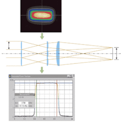
The raw output of an excimer laser is a quasi-rectangular beam, typically around 8 × 20 mm, with a near-Gaussian profile in the short axis, and a “top hat” (super Gaussian) profile in the long axis. Top hat refers to a beam intensity cross section with an extended central plateau that falls off near the edges. One way to transform this into a uniform intensity distribution is a cylinder lens homogenizer, consisting of several individual cylindrical lenslets (see Fig. 1).
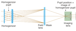
An n-element array of cylindrical lenslets serves to divide the input beam profile into n slices. Each of these input slices is then expanded and mapped across the entire output beam profile, which is accomplished by a second lenslet array and a single reimaging lens. The output beam thus consists of the average of the profile of the individual slices. Separate lenslet arrays are used for the x and y axes because the axes have different intensity distributions and dimensions.
This simple approach provides flexibility in system size, performance, and cost. Increasing the number of lenslets, for instance, cuts the beam profile into more slices, increasing final uniformity. However, a larger number of elements also increases the overall cost and size of the homogenizer. In a typical application, the homogenizer uses 11 or 12 elements for each axis and delivers energy uniformity of 3% to 5% (at 2 sigma) along both axes. In demanding applications such as inkjet-nozzle drilling or silicon crystallization, uniformity is improved to 1.5% (at 2 sigma) by using up to 18 lenslets.
Once a uniform beam has been produced, the next step is to match the beam shape to the requirements of the process. The particulars of how this is accomplished vary tremendously by application.
Thin-line application
One of the most important applications of high-power excimer lasers is flat-panel-display (FPD) annealing at 308 nm. To create the active element of FPDs, a thin layer of amorphous silicon is formed on a glass substrate in a vapor-deposition process. This layer must be transformed into polycrystalline silicon to yield the requisite electrical and photonic properties for high-resolution displays. Until a few years ago, this phase transformation was performed in high-temperature ovens (at 600°C), which required the use of expensive, thermally resistant glass. In addition, the thermal cycling could still cause cracking and yields of less than 100%. Today, virtually all flat-panel silicon annealing is carried out using excimer lasers in combination with low-temperature ovens (200°C), allowing the use of low-cost glass panels.
Typically, large panels are processed and then singulated down to the final display size. The key requirements in this application are uniform irradiation across the entire panel (for consistent processing) and fast throughput. This is accomplished by sweeping a long, thin, highly uniform line across the FPD panel. In one embodiment of this process, each location on the panel is subjected to about 20 consecutive pulses with a fluence of up to 400 mJ/cm2, causing a partial melt of the silicon film. In practice, the length of the projected excimer line is set to be half the width of the panel. Half the panel is then swept under the beam by the supporting table. The table then shifts laterally and the other half of the panel is swept under the beam.
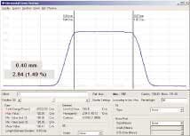
The use of a thin line delivers the high power density required for successful annealing, while enabling fast processing of large-area panels. For instance, one particular thin-line beam-delivery system produces a line profile measuring 370 × 0.4 mm, enabling the latest 740 mm wide FPD panels to be processed with only two sweeps (see Fig. 2). Line lengths of up to 465 mm are possible and are currently moving into production.Photomask applications
Numerous excimer-laser applications require the ability to project a demagnified image of a photomask onto the substrate-to precisely drill an array of small holes, to create a complex mark, or to form MEMS structures, for example. These applications require high-resolution imaging of the mask to produce sharp edges on all the features.
A novel application of this type is the sequential lateral solidification (SLS) process used in the fabrication of thin-film-transistor (TFT) displays—for the latest high-resolution, color screens of Blackberry personal digital assistants (PDAs), for instance. As with conventional FPD processing, this also involves annealing a silicon layer on a glass substrate with a 308‑nm laser. But the SLS process uses a photomask to create a pattern of fine, evenly spaced lines, resulting in a striped pattern of alternating lines of amorphous and polycrystalline silicon (see Fig. 4). These lines are only a few microns wide and must have sharp edges, translating into a spatial resolution of 2 µm for the projected mask image.The beam-delivery and shaping system for this application must correct both axes to properly fill the photomask. This is accomplished using separate cylindrical lens expanders and homogenizers for each dimension of the beam. Next, a projection lens produces a demagnified image of the photomask, such as one reduced by a factor of five, onto the silicon/glass panel. The panel is stepped to process its entire surface.
Some design aspects of the projection lens are worth noting. As previously mentioned, this lens must deliver diffraction-limited resolution for proper feature formation, and also provide high intensity (up to 1 J/cm2). This allows the entire silicon layer thickness to be melted using only two pulses for each location, enabling an entire 370 × 470-mm panel to be processed in just 57 seconds.
The numerical aperture (NA) value for the projection lens must be carefully chosen to balance a number of competing factors. Higher NA produces increased spatial resolution, but also increases lens complexity and cost. Reducing NA makes it simpler to produce a lens with a large working distance, enabling the beam to be projected into a vacuum chamber from outside. Typically, an NA in the 0.10-to-0.13 range provides the best balance of all these factors.
Variable beam-delivery systems
Optimum processing with an excimer beam requires matching the dimensions of the photomask (as well as the pulse energy and the number of pulses per substrate location) to the shape of the area being processed. But, in some cases, these dimensions are not known in advance because excimer lasers are used for a broad range of applications, from marking glass to drilling polyimide to processing ceramics. Those developing new applications may need to vary beam parameters to explore how these affect processing. In these cases, it is useful to be able to adjust the shape, size, and focusing of the beam.
One approach to achieving these adjustments is embodied in the Variolas beam-delivery system from Lambda Physik. Available in several formats, its emphasis is on adjustable performance by using movable and interchangeable components. Most important, the optical components are rail-mounted-movement of the optics effectively changes the power of the demagnifying projection lens without replacing the lens. Similarly, the working distance can be adjusted to meet the specific physical limitations of different applications. Also, by adjusting the relative spacing of the x and y axes lenslet arrays in the beam homogenizer, even the shape of the beam can be altered.
Matching excimer-laser output to the needs of a particular process requires specific beam shaping and focusing optics. However, clever optical and optomechanical design can deliver the required beam transformations within an application’s cost, package, and performance constraints, thus exploiting the full power of UV processing.
Andrew Masters is North American sales manager at Lambda Physik, Ft. Lauderdale, FL, and Thorsten Geuking is product manager at Lambda Physik, Göttingen, Germany; e-mail: [email protected] and [email protected].


