‘New’ UV lasers resolve material and cost issues
From drilling vias in printed circuit boards to scribing brittle low-k dielectrics, solid-state UV lasers are making their mark in microelectronics.
Given their unique ability to process a variety of materials with great precision and very little thermal effect, excimer lasers have become well-respected tools in the manufacture of semiconductor chips, microelectronics, and medical devices. When working with polymers and ceramics, for example, the excimer’s UV wavelengths (157, 193, 248, 266, and 355 nm) are highly absorbed into the target material, resulting in very clean ablation. In addition, a single excimer laser can be tuned to several UV wavelengths simply by changing the optics or gases, making it a very versatile processing tool.
“Excimer lasers are high-order multimode beams, so you are painting with a big, broad brush,” said Jeff Sercel, president of JPSA (Hollis, NH), which offers excimer and diode-pumped solid-state (DPSS) laser-micromachining systems, beam-delivery systems, and materials-processing development. “But you naturally get a very uniform beam, so the excimer is good for step-and-repeat patterning and annealing.”
These features come at a price, however, in terms of both capital equipment and maintenance/replacement costs. In fact, despite their many advantages, excimer-laser systems have found broad adoption in only a handful of industrial applications: microlithography for chip manufacturing; micromachining polymers, ceramics, and glasses; and changing the structure and properties of materials such as oxides, silicon, or glass in bulk or thin films.
“Two things hinder the wide-scale adoption of excimer lasers in industrial processes,” said Corey Dunsky of Coherent (Santa Clara, CA), which offers diode-pumped solid-state UV lasers (the Avia) and a range of excimer lasers through its subsidiary Lambda Physik (Göttingen, Germany). “They are big and expensive, costing hundreds of thousands of dollars, which translates into a very expensive per-square-foot clean-room tool. In addition, the repetition rate of the laser pulses is low (about 4 kHz for photolithography), which slows the material-removal process.”
Even so, because of their larger spot size and higher energy per pulse, excimer lasers continue to find favor in certain applications, particularly those like eye surgery in which the goal is to remove a thin layer of material from a relatively large (millimeter or centimeter) area. But over the last decade, advances in diode-pumped Nd:YAG lasers and beam-shaping optics have resulted in more-robust and lower-cost solid-state UV lasers, which in turn has opened up several new industrial applications for UV laser wavelengths in mass-production environments.1
“In microelectronics, what has sprung up over the last eight to ten years are all these applications where you want to remove material in a very localized fashion, and the diode-pumped solid-state UV laser offers advantages in applications in which you need to focus down to a very localized small spot,” Dunsky said. “With the excimer, to deliver that pulse energy to a very localized area, you have to throw away about 90% of the energy.”
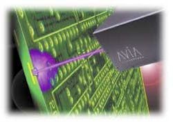
Demand for ever-smaller microvias in IC packaging and flexible circuits, for instance, is driving increased adoption of UV-laser microvia processing systems (see Fig. 1). In fact, drilling vias was the solid-state UV laser’s entrée into high-volume production environments, according to Dunsky, who previously worked at Electro Scientific Industries (ESI; Portland, OR), the company that pioneered laser via drilling in the mid 1990s, first with the CO2 laser and then with an industrial version of a lamp-pumped solid-state UV laser. In fact, there was a synchronicity factor because the laser technology emerged at about the same time that the printed-circuit-board field needed a solution to drilling all these tiny holes.
“The dominant technology for via drilling has been CO2, but with vias going below 60 μm in size, the physics of getting a 10‑μm beam focused below 60 μm is very challenging,” said Ed Swenson, senior vice president of research and development at ESI. “That is why people are moving to UV via drilling, where you can very easily shape the beam down as small as 15 μm.”
Similarly, conventional die-separation processes are no longer practical in terms of throughput and cost; as a result, UV-laser scribing is poised to become a key enabling technology for such applications as blue-LED manufacturing (see Fig. 1). Other emerging UV-laser-based applications in microelectronics processing include laser annealing, drilling and slotting of silicon and III-V materials, scribing ceramics, and dicing MEMS devices. According to Dunsky, applications with some of the biggest near-term potential (in terms of volume production) fall into two categories:
•Thin-wafer dicing. The conventional technology for silicon-wafer cutting is a mechanical diamond saw, which has been around for about 20 to 30 years. But these saws have some problems as the thickness of the wafer decreases, which is important, given the trend toward thinner wafers because of new applications in microelectronics such as smartcards and stacked memory chips. With the UV laser, as the thickness of the wafer decreases, the cutting speed goes up, making it an attractive alternative to diamond saws for volume-production applications.
•Scribing low-k dielectrics. Similar to the processing of memory chips, logic chips have their own set of challenges related to the use of special low-k dielectric materials. In manufacturing, the issue here is the “street” where the saw or laser comes down to cut a wafer into chips. The street contains low-k material that is very brittle and can crack easily when cut with a saw; in addition, the blade wreaks havoc with the metal test structures commonly placed in the streets between the die. While there has been a lot of work by saw manufacturers and chip makers to solve this problem, it turns out the UV laser can easily mitigate the problem, according to Dunsky.
Beam-shaping optics
None of these applications would be possible, however, without key advances in UV-laser technology that have occurred over the last decade. These advances include the industry’s ability to produce very high-quality, lower-cost nonlinear crystals with longer lifetimes, and the shift from lamp-pumping to diode-pumping enabled by the development of more-robust diode lasers that offer lifetimes in the 10,000-hour range (versus lamps, which can only run several hundred hours at a time in a volume-production environment).
One of the most important advances, however, has been the addition of beam-shaping optics. Despite the fact that UV lasers in essence offer virtually heat-free processing, as repetition rates rise and material thicknesses shrink, controlling the size and shape of the beam (and thus the related heat-affect zone) becomes increasingly critical.
“In the UV, there is always an optimum energy density for a certain type of process, but some energy is always left behind. So if you keep raising the rep rate, you risk some melting,” Sercel said. “In most polymers, you start to lose the cooling effects of the laser above 600 Hz, which means you will start to leave residual heat and melting in the material.”
This is where beam shaping comes in. The fundamental TEM00 mode in most lasers is a round beam with a Gaussian intensity profile, a shape that is suitable for many precision laser applications. However, a uniform or “tophat” profile can be more desirable for applications such as photolithography and materials processing because users often want the laser energy distributed uniformly over a round, square, or rectangular area to reduce the heat-affect zone and eliminate such issues as charring.2 Holes drilled in printed-circuit boards with a frequency-tripled Nd:YAG laser at 355 nm, for example, can be drilled faster and more cleanly and sharply with proper beam shaping.
In essence, laser-beam shaping controls the irradiance and phase profile of the output of a laser. The shape of the beam can generally be associated with the irradiance profile, while the propagation properties of the irradiance profile are primarily determined by the phase profile.3 Laser-beam-shaping techniques can be divided into three main classes:
• Apertured beams, in which the beam is expanded and an aperture is used to select a suitably flat portion. The resulting irradiance can be imaged with magnification to control the size of the output beam profile.
• Field mappers, in which the input field is transformed into the desired output field in a controlled manner by bending the Gaussian distributed rays so that they are uniformly distributed in the output plane.
• Multi-aperture beam integrators, in which a subaperture lenslet array divides the input beam into an array of beamlets and applies a phase aberration to each. A beam integrator, or focusing lens, then overlaps the beamlets from each subaperture at the target plane, which is located at the focal point of the primary focusing element where the chief rays of each subaperture intersect.
In some applications, a combination of two of the three techniques is used. In the case of the patented technology developed at ESI, for example, the beam-shaping optics comprise a module that is dropped into the system, instead of incorporating the technology inside the laser chamber. (For more on beam-shaping optics, see “Beam-shaping optics expand excimer-laser applications”.)
“You can’t change the Gaussian nature of the solid-state lasers, but you can put optics in to transform the beam shape to a flat top, and that is what we did at ESI,” Dunsky said. “The key is you want to get the edges of the spot more intense relative to the center.”
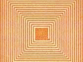
Beam shaping is a critical component of the next-generation UV laser for industrial applications being pursued by ESI. Foremost among these is direct-write laser exposure of photosensitive conductive inks using shaped-beam optics. According to Swenson, in recent years several photoimageable conductive inks and dielectrics have been developed to improve the line- and space-patterning capability of thick-film ceramic circuits. Toward this end, ESI has been working with DuPont to use a UV-laser processing system in conjunction with a photodefinable silver ink to yield patterned traces about 25-µm wide.For example, ESI used a UV laser to photoablate the silver conductive ink to form spaces, resulting in line resolution as fine as 8-µm trace width and 12 µm space width. In another experiment, a 355-nm laser was used to pattern prefired conductive gold ink covered with photosensitive resist material (see Fig. 2). In all of these applications, the processes were performed with a 25-µm Gaussian-shaped laser beam as well as a specially shaped 10-µm tophat square beam; according to ESI, the latter produced finer line resolution with the ablation process but was not as effective for the laser exposure process compared to the Gaussian beam.
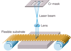
“What is interesting here is if you have a photosensitive material and large areas on a board and you expose the large areas with a standard process and then use the UV Nd:YAG laser to expose the resist, it saves you from having to go to very fine lithography for the whole process.”Similarly, Lambda Physik is using a 308-nm excimer laser in conjunction with gold-plated substrates to produce low-cost PCBs and flex circuits via a laser direct-patterning process that can deliver resolution down to 15 µm. According to the company, this new process requires only nine steps, versus 23 for conventional lithography, and can be used to create flex circuits in a continuous feed, reel-to-reel process with no need for stopped motion (see Fig. 3).
REFERENCES
1. C. Dunsky, Proc. SPIE LASE 2005, published May 2005.
2. D. Brown, K. Kanzler, Laser Focus World 38(8) S11 (August 2002).
3. F. M. Dickey, Optics & Photonics News (April 2003).
About the Author
Kathy Kincade
Contributing Editor
Kathy Kincade is the founding editor of BioOptics World and a veteran reporter on optical technologies for biomedicine. She also served as the editor-in-chief of DrBicuspid.com, a web portal for dental professionals.


