VERTICAL-CAVITY LASERS: Packaging flexibility propels VCSELs beyond telecommunications
The ability to place VCSELs in nontraditional laser packages is changing the way laser sensors are designed and opening new markets.
Jim Tatum
Vertical-cavity surface-emitting lasers (VCSELs) were first realized in the laboratory environment in the mid-1980s, generating a tremendous amount of excitement over potential applications. Technical hurdles, such as heat dissipation, electrical resistance, uniformity of epitaxial growth, and reliability held back the progression of early VCSELs into commercial products. The first commercial VCSEL was introduced by Honeywell (Richardson, TX) in 1996, and since then many of the technical problems associated with aluminum gallium arsenide (AlGaAs) VCSELs have been resolved.1
Explosive growth in fiberoptic data communications, principally driven by the adoption of the Fibre Channel and Gigabit Ethernet (IEEE 802.3z) standards, provided the high-volume market necessary to commercialize VCSEL technology. The data communications market will continue to require ever-increasing bandwidth, with VCSELs providing the migration path to 10 Gbit/s and beyond.2 While this market has and will continue to be a significant growth engine for the VCSEL, it will be complemented by applications in several additional markets.
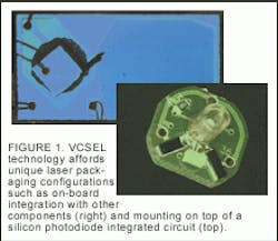
The ability to place VCSELs in nontraditional laser packages is beginning to change the way laser sensors are designed. Like some LEDs, VCSELs emit from the top surface of the wafer. In a custom VCSEL assembly used in a sensing application, for example, a VCSEL is mounted chip-on-board, with an injection-molded plastic lens aligned to the VCSEL to collimate the optical output, as well as a pair of silicon detectors and some passive components. The main points of interest are the high level of integration, the simple lens design (VCSELs have circularly symmetric, nonastigmatic beams), and the small size of the entire sensor. In another assembly technique for VCSELs, the laser is actually mounted on top of a silicon photodiode integrated circuit, something that is not possible with traditional edge-emitting lasers (see Fig. 1). Engineers are beginning to design optical sensors around this type of laser packaging, and penetration into the commercial market will continue the explosive growth of VCSEL technology.
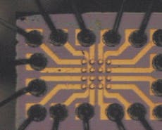
The ease of integrating VCSELs into one- and two-dimensional arrays on a single chip also provides significant packaging advantages. Because the light is emitted from the top surface of the laser, emitting areas are defined to photolithography tolerances, greatly simplifying the alignment of complex optical systems. In addition, various patterns of emitters can be formed via photolithography, potentially allowing the use of pattern-recognition technologies and algorithms in optical sensing. A two-dimensional array of VCSELs can be individually addressed so the optical sensor can be strobed to increase the signal-to-noise ratio or to observe specific patterns in the optoelectronic signal. In a two-dimensional array, a 4 x 4 VCSEL array can be individually contacted (see Fig. 2). One particularly exciting area of application for VCSEL arrays is in laser printing. VCSEL emitters can be fabricated with dimensions significantly smaller than edge-emitting lasers, and the ability to fabricate extended arrays of emitters holds the lure of both higher-speed and higher-resolution laser printing.
FIGURE 2. Two-dimensional 4 x 4 VCSEL array enables individual contacting of elements.
The data communications market also will benefit from the availability of VCSEL array packaging. Linear arrays of emitters are used to transmit data in a parallel fashion, which increases the bandwidth and reduces the need to serialize data. In addition, linear arrays allow amortization of packaging costs over several channels. Two-dimensional VCSEL arrays enable massively parallel free-space optical interconnects for applications such as high-bandwidth switches. Such systems are currently being developed in research laboratories.
A driving force
To date, the commercialization of VCSELs has centered on multitransverse-mode VCSELs operating at 850 nm. The trends observed in the edge-emitting market also will be realized in the VCSEL market: specifically, availability of single-transverse-mode lasers and development of VCSELs operating at other wavelengths. The driving force behind development of new VCSELs will be the laser sensing market. The introduction of oxide isolation in the VCSEL structure has enabled the design of single-transverse-mode VCSELs. For sensing applications in particular, the availability of Gaussian transverse-mode sources is paramount. In laser printing and optical memory applications, for example, one of the most important figures of merit of the optical system is to produce the smallest focused optical spot size. The optical spot size determines the density of optical storage or the resolution of the printed image.
VCSELs operating at visible wavelengths (660-680 nm) have been demonstrated by numerous research organizations, but are yet to become commercially available. While the market volume potential for visible VCSELs is perhaps the highest, the properties of the materials for these sources have made development difficult. Red lasers are grown using the indium gallium phosphide/indium gallium aluminum phosphide (InGaP/InGaAlP) material system grown on GaAs substrates. Because of the relatively small band offset in this material and the consequentially poor carrier confinement, it is difficult to achieve lasing at high temperature. This is especially true in VCSELs where the lasing active volume is quite small in comparison to edge-emitting lasers. In addition, the high aluminum content required to make the lasing mirrors does not provide a large index contrast, which leads to more demands on the epitaxial process. The problems of the material system are exacerbated when moving to shorter wavelengths, such as 630 nm, which are being used for current-generation DVD equipment.
Still, other optical-sensing applications can be addressed with the AlGaAs material system currently being used for 850-nm VCSELs. Oxygen sensing, for example, is typically done with a 763-nm source, and numerous other elements and various compounds have absorption spectra that can be addressed using current commercial VCSEL technology, which ranges from 750-870 nm. Because of the high volume of lasers used in the compact-disk industry, the laser printing industry has developed toner dye that is preferentially absorptive to 780 nm. With the addition of indium to the laser material system (InGaAs), it is also possible to fabricate lasers operating at wavelengths in excess of 1 µm. Longer-wavelength VCSELs have the distinct advantage of operating at a wavelength that is transparent to the substrate, offering an entirely new set of packaging opportunities. Lasers that are transparent to silicon substrates are also possible in this material system, promising yet more packaging flexibility.
Long-wavelength (1300-nm) VCSELs operating in a single spatial mode are highly attractive alternatives to the edge-emitting lasers being used in single-mode fiberoptic communications today. The established infrastructure and excellent reliability of current devices, however, combined with the relatively small-volume market, have slowed the development of 1300-nm VCSELs.
There are significant technical difficulties to overcome in order to produce an all-epitaxial 1300-nm device. Because of the longer wavelength, Auger recombination and free carrier absorption have a large effect on the laser performance. Making matters worse is a very low index contrast in the InGaAsP/InP material system. Other material systems such as GaInNAs and AlGaSb have been attempted as well, with reasonable early results.
Several research groups have demonstrated lasing in VCSEL structures that are not all epitaxial. Among these techniques are the use of dielectric mirrors, wafer bonding the InGaAsP quantum wells to AlGaAs mirrors, and using an optically pumped VCSEL bonded to an 850-nm AlGaAs VCSEL. Each of these approaches brings with it a new set of problems, including reliability, temperature performance, heat dissipation, electrical contacts, and defect densities generated from the wafer-bonding process.
To date, VCSELs have fulfilled their promise as an exciting optical source technology for fiberoptic systems. Because of the much improved parametric optical performance and the dramatic improvement in reliability (more than a hundredfold), the VCSEL has completely replaced edge-emitting lasers in fiberoptic data communication systems. The total number of communications ports using fiberoptics will continue to grow as the need for bandwidth intensifies on the Internet, and VCSELs will continue to be the most effective solution for short-distance multimode fiber links.
Commercialization of AlGaAs VCSELs into other laser-sensing applications is also progressing, with volume markets beginning to emerge in several areas. The future for VCSEL technology is exciting, with rapid growth expected in new applications of current technology, and the emergence of VCSELs at other wavelengths. The inherent advantages of VCSELs will eventually allow them to replace edge-emitting lasers in all but a few applications.
REFERENCES
- J. A. Tatum et al., "Commercialization of Honeywell's VCSEL Technology," Proc. SPIE 3946, 2000.
- J. A. Tatum and K. P. Jackson, "VCSELs Enable High Speed Data Communications," to be published in Lightwave, March 2000.
JIM TATUM is manager of VCSEL technology, Honeywell Sensing and Control, 830 East Arapaho Rd., Richardson, TX 75081; e-mail: [email protected].


