Femtosecond pulses microfabricate diamond
ULTRAFAST LASERS
KANAGAWAResearchers at the Kanagawa Academy of Science and Technology (KAST) have achieved nanometer-scale processing of extremely hard materials such as diamond and sapphire by using femtosecond lasers. This method brings technology one step closer to diamond wafer mounting, eagerly anticipated for next-generation semiconductors. The near-infrared femtosecond Ti:sapphire laser used for the processing emitted at 800 nm, producing pulses with 100-fs duration, energies of 20 to 80 µJ, and a repetition frequency of 1 kHz.
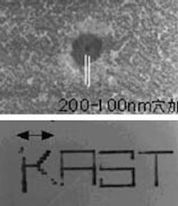
Ultrafast laser makes a 100- to 200-nm-diameter hole in a sapphire crystal (top). The circular area surrounding the hole is bare sapphire, with sputtered gold laying beyond. There is no heat damage to the sapphire crystal in the region surrounding the hole. Similar processing etches fine lines into the surface of a diamond crystal film (bottom). Heat processing usually causes diamonds to oxidize because they are made of carbon; however, there are no traces of burn marks in this sample.
Even materials that absorb only high-energy short-wavelength light can be processed using ultrafast methods that produce highly excited electrons. Conventional laser fabrication inevitably causes damage to the material because the heat of fabrication causes heat relaxation. In contrast, the new method reaches a nonequilibrium state very quickly, so loss due to heat relaxation can be prevented (see figure).
The researchers are collaborating with theoretical groups, because the physics behind this phenomenon is not well understoodthe basic nonequilibrium statistical mechanical theory is still being developed. The stakes are high, as femtosecond lasers may soon be used in large-scale integrated-circuit fabrication.
Courtesy O plus E magazine, Tokyo

