Following the tremendous success of compact-disk (CD) optical storage in the early 1980s, the investment in diode-laser development increased dramatically. Next-generation optical storage systems would require two major improvements to diode lasers: higher power for read/write systems and shorter wavelength to increase data-storage density. Barcode scanning was often cited in the 1980s as a market with large potential for diode lasers with red wavelengths, but the optical storage market at the time was actually about 50 times larger.
To maximize the density of data written by a laser beam, the beam diameter should be as small as possible. The data density decreases with the square of this diameter
D = 1.22 λ / NA
where the numerical aperture (NA) of the focusing objective in a CD storage device is limited by mechanical considerations to less than 0.6. Going from the 780-nm wavelength found in CD storage systems to the 633-nm wavelength of a HeNe laser increases data density by about 50%—not enormous, but a significant improvement.
Better red than dead
Barcode-scanner manufacturers were certainly eager to piggyback onto the development of a red-emitting diode laser. Diode lasers are about 50 times more electrically efficient than HeNe lasers. (One-milliwatt HeNe lasers and diode lasers each draw about the same current, but diodes operate at around 2 V compared to around 100 V for HeNe lasers.) The pricing history of the 780-nm diode lasers, combined with their much smaller size and greater reliability, made visible diode lasers look very attractive to scanner manufacturers.
The first challenge confronting developers was to find a semiconductor with a sufficiently large bandgap. At the time it was thought that larger-bandgap materials tended to have indirect bandgaps.
In indirect bandgap materials, such as silicon, the electrons and holes have, on average, different momenta in the conduction and valence bands, respectively. The energy produced from the recombination of the electrons and holes in such materials is absorbed as heat by the crystal. Direct-bandgap materials, on the other hand, have electron and hole populations with the same average momenta and generate light when the electrons and holes recombine.
Direct-bandgap materials can be formed from so-called "compound semiconductors" in which two or more elements join to form the same crystalline structure as silicon. In the III-V material gallium arsenide (GaAs), for example, the relative absence of an electron (compared to silicon) in the group-III gallium atom is compensated for by the relative excess electron in the group-V arsenic atom. The size of the energy gap and whether it is direct or indirect is determined by the basic properties of the material. Another important material property is the spacing between the atoms in the crystal, which is known as the lattice constant.
No visible means of support
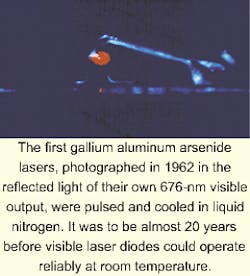
Pure GaAs has a bandgap of 1.42 eV, corresponding to a lasing wavelength of 905 nm. Early diode-laser developers found that mixing aluminum with the gallium to create an alloy for the group-III material results in a higher-bandgap-semiconductor gallium aluminum arsenide (GaAlAs; see photo at top of page). The more aluminum, the larger the bandgap.
In the early 1980s, researchers struggled to manipulate GaAlAs to operate at red wavelengths. Continuous-wave (CW) operation was achieved at wavelengths as short as 680 nm, but the devices were unreliable. Aluminum arsenide (AlAs) by itself is an indirect-bandgap material, as is GaAlAs when the added concentration of aluminum rises above 40%. Even at lower concentrations, the aluminum in the junction region tends to oxidize and bring about the lattice-defect lifetime problems that plagued early diode lasers. Reliable GaAlAs lasers proved to be limited to about what was already available. (The GaAlAs diodes developed for CD players emit at 780 nm.) The claim by manufacturers that the 750-nm-wavelength diodes sold commercially were "visible diode lasers" only served to underscore the fact that these were near-infrared devices.
What was needed was a new semiconductor with a larger bandgap and little or no aluminum. But creating a new compound semiconductor is not simply a matter of substituting one group-III or group-V element for another. The material must be a good electrical and thermal conductor, it should be "hard" in the sense that whatever defects (and dopants) are present, they do not readily migrate through the structure, it needs to accept dopant materials, and so forth.
In particular, the semiconductor must bond to a suitable substrate and to the "cladding layers" that form the confinement regions in heterostructure diodes. This constraint translates to the requirement that the lattice spacing in the different materials be within 0.1% of one another. It is truly remarkable that several direct-bandgap semiconductors meet this criterion. More complex compounds can be engineered to be lattice-matched and yet still have a desirable bandgap (see "Semiconductor design requirements").
The first major success in the visible was the gallium indium phosphide (GaInP) laser produced at NEC and other Japanese companies around 1987. As with earlier GaAs heterostructure lasers, materials for the confinement layers were formed by combining aluminum with gallium to raise the bandgap and lower the refractive index. The device was lattice-matched to a GaAs substrate. These lasers emit at 670 nm and were the first visible diode lasers with reasonable lifetimes.
Black and white and red all over
But scanner manufacturers were concerned that the new red diodes were not red enough. Inks used to encode barcodes were developed for HeNe lasers, and it was thought that many barcodes would not be read by scanners using the 670-nm devices. Modern scanners do use 670-nm diodes, which are now effective because of improved scanning technology and redesigned inks and because the initial concerns about barcode readability were too pessimistic.
If barcode scanning proved to be a more demanding application than diode makers thought, the diodes themselves were disappointing to the scanner makers. Virtually all of the output parameters changed with temperature and age—the power and the aspect ratio of the elliptical beam and its degree of astigmatism—but the major problem was wavelength control. The wavelength of a single diode typically varied about 0.25 nm per degree of device temperature. The same laser in different environments within marketing specifications or at different times in its operating cycle could easily change output color by ±10 nm.
The wavelength also varied from laser to laser, even for diodes cut from the same wafer. Variations between 664 and 694 nm were commonplace. These changes are even discernable to the eye, which as a rule of thumb can distinguish 10-nm gradations in color. The variations originated from the uneven distribution of indium and gallium in the diode material as a result of small fluctuations in process temperature.
In an effort to eliminate performance problems related to temperature changes in diode lasers, efforts continued to shrink the gain region and so reduce the device current. Developers could afford the luxury of shrinking the gain region as a consequence of high gain in semiconductor lasers—in a typical diode laser, light is amplified more than 100 times in a single pass through the 0.5-mm-long cavity.
It was soon discovered, however, that below a junction thickness of about 0.2 µm the threshold current increased rather than decreased in a standard heterostructure. The narrow width of the gain region diffracted the light in the cavity and decreased efficiency. The solution to this problem led to a revolution in the design of diode lasers—the quantum well (QW). All diode lasers being developed today are variations of the QW design.
The basic design principle of the QW is to separate the task of confining the photons from the task of confining the electron-hole pairs. As in the heterostructure, in a QW the junction region for the electrons and holes is bounded by a higher-bandgap material, but these layers no longer serve to confine the photons by total internal reflection. The higher-bandgap material has a refractive index matched to the junction region, and photon confinement is performed by more widely separated layers of material with a lower index of refraction. The junction region can now be made extremely thin without refracting the laser light out of the cavity.
The QW structure results in several other more profound effects in semiconductor lasers. The submicron size of the confined dimension (actually less than 50 nm thick) causes the semiconductor bandgap to split into discrete sub-bands that serve to further lower threshold current, increase gain, and improve beam coherence. The thinness of the layers also relaxes the constraint on lattice matching.
Quantum wells were first demonstrated by Holonyak at Bell Labs (Murray Hill, NJ) in 1978 in a tour de force using liquid-phase epitaxy (LPE), but the development of new structures had gone beyond the capabilities of the venerable LPE process. New fabrication techniques were required before QWs could become commercially feasible in the 1980s, notably molecular-beam epitaxy and metal-organic chemical-vapor deposition (see Fig. 1).Just as with GaAs, shorter wavelengths in GaInP can be obtained by adding aluminum to the active layer, and it will cause the same reliability problems without advancements in design related to QWs. Using the newest fabrication techniques and QW structures, however, Philips Semiconductor was the first to demonstrate the long-sought 633-nm wavelength using GaAlInP in 1990 and, along with other companies, offered the diodes commercially in 1993. Such lasers are sufficiently reliable for use in digital video disks (DVDs).
The thirst for higher data-storage densities continues to fuel the development of diode lasers at still shorter wavelengths.
ACKNOWLEDGMENTS
We would like to thank the following individuals and organizations for providing images used in the Semiconductor Lasers 2000 series timeline: Michael W. Davidson, Florida State University; GE Research and Development Center; Zhores I. Alferov; Nick Holonyak, University of Illinois; Dan Botez, University of Wisconsin-Madison; Lucent Technologies, Bell Labs; Connie Chang-Hasnain, University of California Berkeley; Nichia Chemical Corporation; Jack Jewell, Picolight Corp.Ed.
Next month this series will discuss higher-power visible lasers and lasers at other colors.
Semiconductor design requirements
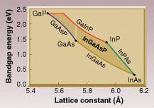
Simplified plot shows the bandgap energy vs. lattice constant for compounds of the group-III materials gallium (Ga) and indium (In) with the group-V materials arsenide (As) and phosphorous (P). Similar diagrams exist for other combinations of elements. It shows how crystal growers can design a semiconductor to meet requirements for both lattice constant and bandgap energy.
The black dots at the corners of the figure represent the simple binary compounds of the selected materials. The value of the lattice constant is a result of the size of the constituent elements. Indium is a larger atom than gallium, for example, so InAs has a larger lattice constant than GaAs.
The colored lines show the variation of bandgap energy and lattice constant for the so-called ternary compounds, which can be thought of as connecting the binary compounds. The difficulty of lattice-matching a material of interest to a substrate can be better appreciated when it is realized that there are only a handful of suitable substrates available even for developmental work.The means to achieve greater freedom in wavelength selection is to add another element to the mix and form a quaternary compound. Adding phosphorus to InGaAs for example will raise the bandgap. Because it is a smaller atom than the arsenic it partly replaces, it also shrinks the lattice. By adding additional (large) indium atoms to the compound to replace (small) gallium atoms, the crystal grower can offset the shrinking effect of the phosphorous and keep the lattice constant at the desired value.
In this way quaternary compounds can achieve the entire range of bandgap energies and lattice constants of the related binary compounds. The shaded area represents the range of these parameters for the quaternary compound InGaAsP. The range of bandgap energies available for InGaAsP with a lattice constant that matches a GaAs substrate is shown by the vertical white line.
About the Author
Stephen J. Matthews
Contributing Editor
Stephen J. Matthews was a Contributing Editor for Laser Focus World.


