Semiconductor Lasers: Phase-modulating semiconductor laser projects 2D beam patterns without HOEs or SLMs
In 2016, researchers from Hamamatsu Photonics (Hamamatsu City, Japan) developed a chip-scale semiconductor laser that is capable of projecting 2D beam patterns directly from the gain medium, without requiring external holographic optical elements or spatial light modulators.1 Since then, the researchers have continued to improve the technology, and recently were able to produce 2D patterns without the surface-normal spot beam that was hindering adoption of the technology.2
2D pattern-projection laser overview
The beam quality of most semiconductor lasers is much poorer than their external-cavity counterparts. However, semiconductor photonic-crystal surface-emitting lasers (PCSELs) have high beam quality because of the ability to tailor the properties of the resonating photonic-crystal structure.3
To project a pattern from the lasing cavity itself, the device is fabricated with an active phase-modulating resonator layer sandwiched between the n-electrode (at the top) and p-electrode (at the bottom) layers placed on an open heat sink. The modulating layer consists of an array of air holes that are locally shifted from a periodic photonic crystal according to a phase distribution that produces the desired grayscale image or other 2D desired pattern.
This integrable phase-modulating surface-emitting laser (iPMSEL) allows concurrent lasing and phase modulation to produce a 2D pattern of emission in the far field from an 800 × 800 µm chip with a 1400 × 1400 array of holes for lasing and for phase modulation.
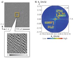
The phase distribution is the inverse Fourier transform of the bitmap image of the desired beam pattern, and is obtained using Mathworks or MATLAB software and the ifft2 function (see figure). Output power for this iPMSEL exceeds 500 mW at a 930 nm emission wavelength, which can be tuned by device design.
For the laser that generated the “iPM Lasers” output, there is a bright surface-normal spot at the center of the emission pattern. The researchers discovered that this surface-normal (zeroth-order) beam corresponds to components of vertical diffraction of the band edge modes of the photonic crystal layer without spatial phase modulation. To remove this zeroth-order beam, the lasing cavity was modified with a structure that prohibits vertical diffraction of the band edge modes.
However, this process also prohibits the vertical emission of the target beam pattern. To address this issue, a checkered-pattern phase shift that shifts the target beam pattern from the in-plane to the vertical direction is added to the original phase distribution. As a result, the surface-normal beam is eliminated from the target beam pattern. This also sends more light energy into the far-field illumination of the 2D beam pattern, as the surface-normal zeroth-order energy is suppressed.
“The iPMSEL is a quite promising semiconductor laser because it can emit arbitrary beam patterns from a chip-sized device. This compactness is suitable for integration; in fact, it could easily switch the beam patterns from an array of iPMSELs integrated into one chip,” says Kazuyoshi Hirose, researcher at Hamamatsu Photonics. “We believe that the iPMSEL will be extremely useful in structured illumination applications such as superresolution microscopy, 3D sensing, and lidar. In the future, if the large-scale integration of iPMSELs is realized, it could be the basic component of a 3D display device.”
REFERENCES
1. Y. Kurosaka et al., Sci. Rep., 6, 30138 (Jul. 26, 2016).
2. K. Hirose et al., Opt. Express, 26, 23, 29854–29866 (2018).
3. M. Imada et al., Appl. Phys. Lett., 75, 3, 316–318 (1999).
About the Author

Gail Overton
Senior Editor (2004-2020)
Gail has more than 30 years of engineering, marketing, product management, and editorial experience in the photonics and optical communications industry. Before joining the staff at Laser Focus World in 2004, she held many product management and product marketing roles in the fiber-optics industry, most notably at Hughes (El Segundo, CA), GTE Labs (Waltham, MA), Corning (Corning, NY), Photon Kinetics (Beaverton, OR), and Newport Corporation (Irvine, CA). During her marketing career, Gail published articles in WDM Solutions and Sensors magazine and traveled internationally to conduct product and sales training. Gail received her BS degree in physics, with an emphasis in optics, from San Diego State University in San Diego, CA in May 1986.