VCSELs are fully integrated into and planarized with silicon CMOS ICs

Researchers at the Massachusetts Institute of Technology (MIT; Cambridge, MA) have integrated 850-nm-emitting gallium aluminum arsenide (GaAlAs) vertical-cavity surface-emitting lasers (VCSELS) into silicon CMOS integrated circuits (ICs) in such a way that the VCSELs are planarized (resulting in compatibility with full 300-mm-diameter wafer processing) and have threshold currents and thermal characteristics similar to VCSELS left on their native GaAs substrates. Potentially useful for optical interconnects or as optical sensors, the integrated lasers are also compatible with bump-bond processing and three-dimensional integration.
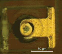
The oxide-aperture VCSELs are fabricated as stand-alone “pills” 55 µm in diameter, but are otherwise similar to standard VCSELs; the lasers are then placed in recesses in the IC. After the pills are solder-bonded in place, a layer of benzocyclobutene and a layer of silicon dioxide are deposited on the IC, encapsulating the VCSELs and replanarizing the chip. After etching contact vias, metal is deposited on the surface and the remaining interconnects patterned. Typical continuous-wave threshold currents vary from 1 to 2.5 mA; this variability can be reduced by dry-etching rather than wet-etching the VCSEL mesas. Contact Clifton Fonstad at [email protected].