Terahertz Sources - Laser advances drive THz photoconductive source technology
ELLIOTT R. BROWN
Near-infrared semiconductors and fiber lasers continue to improve in performance while their costs decrease, driven largely by worldwide growth in the fiber-optic telecommunications industry. Consequently, commonly available single-spatial-mode 780 to 1550 nm diode lasers at 100 mW meet the temporal and spatial-coherence requirements of photomixing down to the terahertz region and below. And continuing improvements in erbium-doped fiber-amplifier technology, combined with improvements in fiber-coupled nonlinear optics (second-harmonic generators, for example), have enabled 800 nm modelocked lasers with 10 mW average output power and peak power above 1 kW. As such, these lasers meet the temporal and power requirements of photoconductive switching for terahertz time-domains systems now used worldwide.
The interest level and size of the terahertz community has grown significantly in recent years because of new phenomenology in biology and chemistry such as molecular absorption signatures, new solid-state sources such as quantum-cascade lasers, and timely system applications such as concealed-object imaging and explosives detection. At the same time, engineers still find the terahertz region to be one of the most challenging across the electromagnetic spectrum for several reasons, one of which is the lack of broadband, affordable, room-temperature instrumentation.
Ultrafast photoconductive devices represent one of the most successful developments in the history of the terahertz field. Photoconductive switches have become the preferred device for generation of broadband terahertz radiation in a multitude of applications, particularly low-resolution spectroscopy and imaging. Starting with the pioneering work of David H. Auston, these switches have steadily improved in performance with a giant leap occurring in the 1990s with the development of low-temperature-grown (LTG) gallium arsenide (GaAs).1, 2 Although less common, photoconductive mixers (photomixers) have also been developed for device applications requiring continuous-wave single-frequency output and wideband tuning, such as in high-resolution spectrometers and tunable local oscillators. The primary shortcoming of the photoconductive devices has always been average output power, limited to less than 100 μW in switches and approximately 1 μW in photomixers. Through steady development in the photoconductive devices and the commercial lasers that drive them, performance has improved and photoconductive-based terahertz systems have become much more affordable.Terahertz photoconductive materials
For more than a decade there has been great interest in “defect engineering” semiconductors to achieve subpicosecond photocarrier recombination, high-breakdown electric fields, and other effects useful in terahertz photomixers and fast photoconductive switches. Much of this interest involves LTG GaAs and the role of excess-arsenic precipitates.3 As a result, a new approach has been developed involving compound semimetal-semiconductor nanoparticles grown at normal temperatures. Experience shows that the growth of thin layers of erbium arsenide (ErAs) in GaAs leads to the formation of disk-like ErAs nanoparticles with subpicosecond lifetimes similar to those in LTG GaAs.4 In a separate development, terahertz photomixers have been developed having record-high terahertz output power, particularly at frequencies beyond 1 THz.The photomixer power spectrum can be understood in terms of the morphology, band structure, and semiclassical transport principles applied to the semimetal-semiconductor nanocomposites. The key morphological aspect is that during growth the ErAs layers tend to disintegrate into isolated ErAs nanoparticles having greater size than the typical GaAs point defect. This shows up clearly in transmission electron micrographs and has been reported in separate studies. For example, growth at 630°C shows that the deposited ErAs forms isolated islands, which are about 0.9 to 1.2 nm high and extend over a broad range up to around 10 nm in the lateral dimensions.
To mitigate impact ionization and other breakdown effects, the ErAs:GaAs has recently been improved. The key difference is the spatial distribution of the ErAs nanoparticles. In previous material, the nanoparticles were distributed in quasi-two-dimensional layers because of the ease in creating such layers by molecular-beam epitaxy. In the current material, the ErAs nanoparticles are nominally distributed homogeneously by codepositing the Er along with the Ga and As. This approach mimics what occurs with arsenic precipitates in LTG GaAs, but maintains the superior transport in the GaAs between the nanoparticles.
Sweep oscillator application
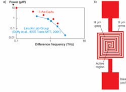
As a result of its intrinsic high-frequency response, the photomixer can generate useful levels of power in the terahertz region provided it is designed for efficient external coupling of its two optical pump lasers, with good thermal management of the absorbed laser power. For an ErAs:GaAs interdigital device driven by two frequency-offset external-cavity diode lasers centered around 775 nm, the active region of the photomixer is located inside a resonant optical cavity having a distributed Bragg reflector (DBR) below and a silicon-nitride-based antireflection coating on top (see Fig. 1).5 With this design, the average power from each pump laser can be increased up to about 30 mW before the device fails. The terahertz output is coupled through a square spiral antenna and into free space using a high-resistivity silicon hyperhemispherical lens.
The maximum terahertz output power from the photomixer is about 10 μW at the low-frequency end (100 GHz), just above 1 μW at 1 THz, and then begins to fall off as expected. These values represent a factor-of-two improvement over previously reported maximum output power levels from LTG-GaAs photomixers.6 These power levels were measured using a Golay cell whose responsivity was (cross) calibrated at 104 GHz using a waveguide-mounted Gunn diode, thermal power meter, waveguide attenuators, and a standard-gain feedhorn. The calibrated Golay cell responsivity is less than its mid-IR responsivity because of lower external power coupling, as expected.
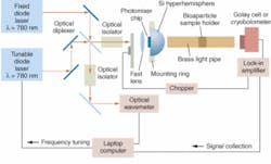
Although low by microwave standards, the power of these new ErAs:GaAs devices is high enough for them to be used in a free-space-coupled terahertz sweep oscillator for device and materials transmission studies in the terahertz region for bioparticles and biomaterials (see Fig. 2). The setup requires no large gas lasers, high voltages, or large magnetic fields, and it can operate in an “all-room-temperature” mode using a Golay cell as the detector, which provides an average signal-to-noise ratio of about 20 dB between 100 GHz and 1 THz. Operation with substantially higher signal-to-noise ratio can be obtained with terahertz cryogenic bolometers.Switch design and characterization
Compared to photomixers, photoconductive (PC) switches have slightly different design considerations with high direct-current voltage standoff as a primary consideration. As such, the active epitaxial layer in the PC switch is best made thick without a DBR or similar structure below it, since such structures tend to impair high-bias reliability. A typical design consists of a 1.5-μm-thick film of ErAs:GaAs grown on a Al0.9Ga0.1As heat-spreading layer on a semi-insulating GaAs substrate. A second aspect of PC switch design, and photomixers alike, is the terahertz radiation coupling structure to a low-loss transmission line or free space. The current design is the same square spiral of the previously described photomixer, whose small periphery allows it to couple short terahertz pulses to free space with low dispersion, attenuation, and time delay.
Thanks to 1.55 μm erbium-doped fiber technology, ultrafast modelocked lasers are now available with 200 fs pulse widths and more than 100 mW average-power levels. This is enough peak power to drive a second-harmonic generator (SHG), producing subpicosecond pulses centered around 793 nm and having an average power of approximately 22 mW.7 The pulsewidth can be estimated from the spectral bandwidth, Δλ = 5.36 nm, measured with a grating spectrometer, which corresponds to a 3 dB bandwidth of Δν = 2.56 THz at the peak wavelength of 793 nm. The corresponding pulsewidth is then approximated by Δt ≅ 1/Δν = 390 fs, which includes all dispersive and distortive effects from optical fibers and the SHG itself. The 793 nm pulses are focused on the PC switch while it is biased with a low-noise constant-voltage power supply.
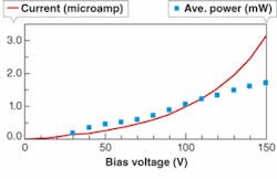
The terahertz output beam is coupled to free space through a silicon hyperhemisphere, and the average power is measured with a commercial thermopile power meter (see Fig. 3). Results from the calibration of the thermopile suggested that thermopiles are more useful in the subterahertz region than people may have thought.Another important factor is saturation of the free-space-coupled terahertz thermal detectors previously used to measure terahertz power. Thermopiles are famous for their large dynamic range and the ability to accurately measure the average power of pulse trains having very high peak power Ppeak, such as the output from Q-switched Nd:YAG lasers. The peak terahertz power Ppeak from the photoconductive switch is more difficult to measure than the average power, but can be roughly calculated as approximately 33 W at the 150 V bias point. This is an impressive number for the terahertz region.
REFERENCES
1. D.H. Auston et al., Phys. Rev. Lett. 53, 1555 (1984).
2. B.B. Hu et al., Phys. Rev. Lett. 67, 2709 (1991).
3. F. W. Smith et al., IEEE Electron Device Lett. 9, 77 (1988).
4. C. Kadow et al., Appl. Phys. Lett. 75, 3548 (1999).
5. J.E. Bjarnason et al., Appl. Phys. Lett. 85(18) 3983 (2004).
6. S.M. Duffy et al., IEEE Trans. Microwave Theory and Tech. 49, 1032 (2001).
7. E.R. Brown et al., Rev. Sci. Inst. 75, 5333 (2004).
Tell us what you think about this article. Send an e-mail to [email protected].
ELLIOTT R. BROWN is a professor in the Electrical and Computer Engineering department at the University of California, Santa Barbara, Santa Barbara, CA 93106; e-mail: [email protected]; www.ece.ucsb.edu.


