Extreme-UV sources are on track for next-generation chip manufacturing
With semiconductor-chip manufacturers already pushing the limits of optical lithography, it is not surprising that the vendors that design and build these systems are hard at work on the next generation of microlithography: extreme ultraviolet (EUV). And if these toolmakers stay on track with their technology development roadmaps, EUV lithography will be well positioned to displace its excimer-laser and deep-ultraviolet (DUV) predecessors in the next three to four years.
By most accounts, current optical-lithography techniques have been extended about as far as they can go. Many installed systems use 248-nm (krypton fluoride) or 193-nm (argon fluoride) excimer-laser sources to print 100-nm features on chips in volume production. But the push to further improve computer-processing speeds has chip manufacturers clamoring for sub-50-nm features sooner rather than later, and 157-nm fluorine (F2) technology appears to be the near-term—albeit short-term—solution.
Originally, F2 laser technology was slated for insertion at the 100- and 70-nm nodes this year, with EUV lithography poised to take over at the 45- to 30-nm node between 2005 and 2007. But F2 laser lithography still has hurdles to overcome before it is ready for high-volume production, including the ready availability of calcium fluoride for optics and the contamination of optical elements. Thus, toolmakers have opted to push the capabilities of 193-nm lithography to meet current production needs and control costs while they work to refine their 157-nm products.
"You have to look at this in terms of industry requirements, which have changed quite a bit in the last few years," said Richard Walker, president of TRW-Cutting Edge Optronics (St. Louis, MO), a subsidiary of Northrup Gruman Space Technology that is developing a high-power diode-pumped Nd:YAG laser source for EUV lithography. "ASML, Canon, and Nikon have told us they need a certain amount of power to get the throughput that end-users are demanding, but every time they increase the power requirements, they are really pushing the limits of the technology."
These dynamics actually bode well for the future of EUV lithography, and efforts to develop and commercialize 13.5-nm lithography are well under way. Spearheading this effort has been the EUV LLC Consortium (Livermore, CA), which was established by Intel (Santa Clara, CA) in 1997 and funded by more than $250 million in industry investment (see "EUV consortium blazes collaboration trail"). International Sematech (Austin, TX) has served as another collaborative forum for EUV developers, sponsoring the first International Symposium on EUV Lithography last October and several related workshops. According to most chip-equipment-manufacturer roadmaps, EUV lithography should be ready for insertion at the 45-nm node by 2007, with the first beta systems in place by 2005.
"The industry will try to extend 157 as far as possible, but 157 is very limited in terms of the number of technology nodes it can support," said Chuck Gwyn, general manager and program director of the EUV LLC Consortium. "If you try to stretch it farther, it is extremely expensive."
Power, debris, and cost
While the basic science is in place and most companies are on track with their technology-development roadmaps, there are still many obstacles to overcome before EUV will be ready to replace F2 lithography in a production environment by 2007. According to the 300-plus attendees at Sematech's EUV symposium in October 2002, source output power tops the list of the 10 most critical issues in EUV lithography development, followed by defect-free multilayer mask blank manufacturing, source and optics reliability, and cost of ownership.
"The last few technical conferences on EUV have focused on the fact that the light source is the most critical challenge to be solved," said Bob Akins, CEO of Cymer (Carlsbad, CA), a leading provider of laser-based lithography systems. "All the optical components used in building such a tool are reflective. So to overcome the optical losses, you have to have a source that has the right wavelength and is very intense."
Simply put, EUV lithography differs from excimer-laser and DUV lithography in that instead of using a laser to directly etch the patterns onto the chips, it uses optical or electrical energy to heat a donor material—most often xenon—to a very high temperature, forming a plasma around 13.5 nm that is used to etch the patterns. At this point, developers are focusing on two plasma-based approaches: laser-produced plasma (LPP) and discharge-produced plasma (DPP). Both have their pluses and minuses; for the time being, the primary development goals involve creating the output power necessary for production-level EUV lithography at levels below 50-nm and reducing the debris generated in the process.
"A few years ago we thought we only needed 15 to 20 W of output power, but now the view is that we need 80 to 120 W," said Akins. "And this power needs to be delivered to the right place, with the right spectral characteristics, and it has to be clean."
Thus, while source output power is a key consideration, so is power at the point of collection and the production of debris in the process. These points have become important differentiators in the race to develop LPP and DPP systems for EUV lithography, along with the overall cost of each type of system.
According to LPP proponents, the primary disadvantage of a discharge source is the production of debris between the electrodes, which results in the need for a debris mitigation system. In addition, the production of excess peripheral heat requires a spectral filter and other thermal management capabilities. An LPP system, on the other hand, does not require spectral purity filters or debris mitigation filters. In addition, because the plasma is produced a long distance from the source, the hardware does not thermally destroy any particles.
"The three main advantages of an LPP system are no debris, spectral purity, and efficient collection," Walker said. "Those three things give you significant advantages in the amount of power you collect as well as the amount of power you generate."
The race is on
Discharge-plasma developers beg to differ, however, citing the complexity and cost of a laser-based system, which they say will be up to three times as much as gas-discharge systems. According to Akins, whose company has an aggressive commercial DPP development program, to scale an LPP system to the very high powers needed for production tools is a major undertaking, requiring numerous lasers clustered around the gas jet and frozen xenon target.
"We are high-power laser experts, but years ago we examined the LPP technique and discarded it in favor of DPP," Akins said. "The discharge techniques can be much simpler and even offer scalability to high power levels."
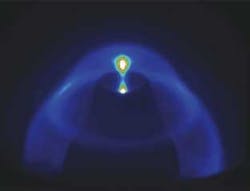
Cymer's dense-plasma-focus (DPF) technique uses a coaxial electrode arrangement to create plasma in low-pressure xenon gas. Electrical current is then used to accelerate the plasma to very high velocities and create the "pinch" (see Fig. 1). According to Akins, DPF has the advantage of producing very efficient pinch for very efficient radiation and grabbing half the light it emits. In addition, the system can be run at very high repetition rates—currently 2000 pulses/s and eventually, Akins says, 10,000 pulses/s. Cymer has six prototype EUV sources up and running and has demonstrated the ability to produce 5 W of collectable EUV power and about 27 W collected clean power. The company expects to deliver its first prototype unit by the end of 2004.
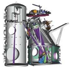
At this point, however, LPP has a leg up in terms of commercialization, in large part because the bulk of the work in EUV source development has been in LPP. The first beta system, which came out of the EUV Consortium, was demonstrated at Sandia National Laboratories in April 2001 (see Fig. 2). The prototype Engineering Test Stand (ETS) is now being used by LLC partners to refine the technology and develop commercial EUV systems.
Because of its role in establishing the consortium, Intel had "first choice" on much of the ETS technology. According to Gwyn, Intel has been using the ETS system to evaluate the feasibility of EUV and optimize its production. The company expects to have beta tools in 2005 and commercial systems by 2007.
"Intel is a little more aggressive than many of the other companies in putting the new technologies in our fabs," Gwyn said. "Our goal is to implement EUV lithography in 2007 for the 50-nm node and then extend it to the 30- and 20-nm nodes—basically to the end of when silicon can be used for chip manufacturing in its present form."
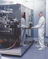
Cutting Edge Optronics is also well ahead in the development of its prototype EUV system, having demonstrated last October the highest output power from an EUV source—12 W. By December 2002, the company had improved that output to more than 20 W, and Walker believes they will demonstrate 4.5-kW output with 1% conversion efficiency this year (see Fig. 3). In the mean time, the company is working on a new laser that will provide 12 kW of output power.
Cost of ownership
But Walker is quick to point out that the bigger issue in EUV lithography is cost of ownership. Because the power requirements keep going up, the source is becoming increasingly expensive, and the need to print more detail per wafer per dollar per hour is putting pressure on source manufacturers—the cost of the source represents 10% to 15% of the overall system cost. Given that commercial EUV systems are expected to cost $20 million to $60 million each, that percentage is significant.
"Right now, tool manufacturers are demanding the ability to produce 100 wafers/hour, so source manufacturers are being pushed to produce more and more but make it cost less and less," Walker said.
In the long run, Akins says, the final issue in the adoption of EUV lithography is going to be system reliability and operation costs. "It is not a matter of whether EUV will happen, but how soon and how competitive it will be in terms of throughput and costs," Gwyn said.
EUV consortium blazes collaboration trail
Established by Intel in 1997, the EUV LLC Consortium comprises the major U.S. chip manufacturers and semiconductor equipment providers, including Motorola, Advanced Micro Devices, Micron Technologies, Infineon Technologies, and IBM. Through the EUV LLC, private industry has funded 100% of the EUV lithography research in the United States. This work resulted in the first beta EUV-lithography test system, demonstrated at Sandia National Laboratories in 2001.
Europe and Asia have several EUV efforts under way as well. In Europe, the MEDEA+ program is supporting about a dozen EUV-related projects and is coordinating commercial and academic developments in EUV tools, sources, masks, and imaging. Germany is expected to spend $50 million between 2001 and 2004 on R&D programs that involve German-based makers of EUV infrastructure components. The first commercial EUV system is likely to come from ASML (Veldhoven, The Netherlands), which reportedly will have a beta system up and running by 2005.
Several Japanese universities and private companies have organized an EUV association (EUVA), and the government is coordinating a cooperative EUV-source program involving Komatsu, Ushio, and Gigaphoton. Competitive forces have also prompted Canon and Nikon to collaborate on a beta EUV-exposure tool that reportedly will be ready by late 2005. In South Korea, the Ministry of Industry and Energy has formed a 10-year EUV program, with the goal of developing an alpha tool by 2008.
"If it hadn't been for the EUV Consortium, EUV lithography wouldn't be on anyone's roadmap today," said Chuck Gwyn, general manager and program director of the consortium. "When we started in 1997, two to three labs were working on some experiments. Today, 150 companies are involved in some aspect of EUV lithography and Europe, the United States, and Japan all have major EUV initiatives in place."
About the Author
Kathy Kincade
Contributing Editor
Kathy Kincade is the founding editor of BioOptics World and a veteran reporter on optical technologies for biomedicine. She also served as the editor-in-chief of DrBicuspid.com, a web portal for dental professionals.