Lasers etch elegant patterns in flat-panel displays
Laser patterning in microelectronics manufacturing is not a new concept. In the 1980s, excimer lasers were used to pattern indium tin oxide (ITO) coatings on computer touch screens and for making slot antennas (a radiating element formed by a slot in a conducting surface or in the wall of a waveguide) on certain minivans. In recent years, laser-based patterning and thin-film removal processes have begun to find favor in the production of flat-panel displays, driven in large part by the emergence of large-area displays that require precise, accurately defined patterns for electrical circuits.
Laser micropatterning offers a cleaner, more efficient alternative to conventional chemical-etching processes for creating pixels, conductors, insulators, vias, and other patterns in glass, plastic, and other dielectric materials used in fabricating liquid-crystal displays (LCDs), plasma panel displays (PDPs), and even organic light-emitting diode (OLED) displays. The laser process is scalable and can yield smaller, more-precise patterns, an important advantage as display makers push for higher resolutions in both smaller (cell phones and handheld computers) and larger (high-definition TVs) form factors.
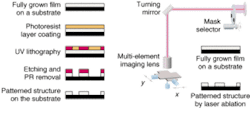
As in the manufacture of integrated circuits, the accepted method of patterning large flat-panel displays is a five-step, multiple-system, photographic process involving photoresist coating, exposure, developing, wet chemical etching, stripping, and baking. The exposure step may require a photomask, produced also by multistep wet chemistry.
Laser micropatterning, on the other hand, is a single-step, dry process sometimes conducted in a nitrogen environment (see Fig. 1). The laser beam etches away the overlying polymer, ITO, or thin-film metal from the glass or polymer substrate without damaging the substrate itself. The laser energy breaks the material's bonds, causing the vaporized material to be ejected into the collection path of the debris nozzle and carried away from the substrate. These advantages have prompted display manufacturers around the world to begin adopting laser-based thin-film removal in LCD production and to consider these systems for next-phase PDP production.
Excimer vs. solid-state
Two types of lasers are currently used for patterning flat-panel displays: excimer (or other ultraviolet) and solid-state (primarily diode-pumped Nd:YAG at 1064 and 532 nm). Each brings its own advantages—and applications—to the table.
Ultraviolet lasers, for example, are good for large-area treatments of substrates or for imaging shapes onto various kinds of dielectric materials because they have a large-area beam that can be used to pattern features, much like a stepper system. In essence, the UV process cleanly removes the thin film from a substrate with less energy than would be required to vaporize the equivalent volume of film. As a result, excimer and other UV lasers are finding application in patterning transparent conducting oxides with electrodes or other features, machining layers in polymer and OLED devices, and drilling interconnects and vias for multilayer systems.
"When working with thin films, the UV energy is absorbed in the film and transmitted through it, ablating the adhesion layer in the process," said Jeff Sercel, founder and president of JPSA Laser (Hollis, NH), a developer of excimer-laser technology for micromachining applications. "If the film is thin enough, the heat transfer allows the energy to be absorbed and transferred through in one pulse, so the process is very efficient and covers a very large area."
According to Sercel, another advantage of the excimer is that the various wavelengths—248, 308, and 351 nm—make it possible to customize the wavelength to the application, the dielectric, and the substrate. "Being able to choose between the different wavelengths allows better selective material removal for patterning," he said. "If you are trying to remove ITO from a glass substrate, for example, and that substrate absorbs strongly at 248, you might want to use 308 or 351 nm. And if you have a very sensitive substrate and want to make an ITO pattern that is very clear, you might pick a longer wavelength."
But when it comes to micropatterning, the excimer also has its drawbacks, primarily in terms of cost and speed. As a result, solid-state lasers have also found their place, particularly in ultra-high-speed patterning for displays. The high repetition rate of diode-pumped solid-state lasers such as the Avia from Coherent (Santa Clara, CA) make them more appropriate for direct writing of intricate, nonrepeating patterns. While these lasers do not offer the same power levels or resolution as the excimer, they do have good average powers and very high frequencies, which means they can achieve similar process parameters with higher process rates.
"The excimer is very good because you have a large beam and you can image down through the slot and traverse over a plate and slowly ablate the filters, patterning each of the colors," said Todd Lizotte, vice president of R&D at NanoVia (Londonderry, NH). "The problem with the excimer is that it can only run up to 200 Hz. There are kilohertz versions, but they don't have enough average power to allow you to pattern effectively and efficiently."
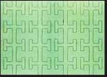
Exitech (Oxford, England), a systems integrator with a long history in excimer- and solid-state laser micromachining, is currently using diode-pumped Nd:YAG lasers to do pixel patterning in PDPs (see Fig. 2). According to Adrian Baughan, sales and marketing manager at Exitech, there is a good match between ITO and the diode-pumped Nd:YAG in terms of absorption. In addition, Exitech uses fiber delivery to keep the laser source remote from the machining process, which is an advantage in terms of reliability in a production environment. The company recently introduced the PixAblater family of dry-etching tools for PDP manufacturing, incorporating the company's FocaFloat optic head to ensure that the substrate surface stays in focus despite variances in substrate thickness. According to Baughan, the PixAblater can process up to 80 42-in. PDPs per hour.
"We are concentrating first in plasma displays because we can do large panels very quickly," Baughan said. "It is thought that smaller screens will be exclusively LCD and the larger will be PDPs because it will be cheaper to manufacture large PDPs vs. large LCDs."
OLED displays
Looking even further ahead, most of the display manufacturers—and their consumer-electronics customers—are actively developing or evaluating OLED technologies for their next-generation products. According to the research firm iSuppli/Stanford Resources (El Segundo, CA), the worldwide market for OLED displays is expected to grow from $91 million in 2002 to $215 million in 2003 and $3.1 billion by 2009. The first active-matrix OLED product—a digital-camera back display from Kodak—was released in March, and OLED cellular phone displays are expected later this year from Sanyo Electric.
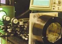
While this market potential represents an attractive opportunity for new manufacturing technologies, it is unclear what role lasers will play. Some proponents believe that laser-based processes easily lend themselves to OLED patterning, while others say that lasers are better suited for dye transfer than micropatterning of OLED dyes and substrates (see Fig. 3). Not only are there unique challenges to using lasers with organic polymer-based materials, but competing techniques such as inkjet printing appear to have a leg up in being closer to commercialization in a production environment.
"At DuPont, we are currently using laser-based techniques for micropatterning and thin-film removal in our OLED displays, but we have significant concerns about using lasers for mass production because it is a difficult process to control and it creates particulates, which are bad in any microdimension process," said Tom Miller, president and general manager of the passive-matrix business at DuPont Displays (Research Triangle Park, NC).
As a result, DuPont and its competitors are looking at alternative patterning approaches such as inkjet printing, in which the organic dye is applied in specific patterns on the substrate vs. being applied across the entire substrate and then selectively ablated. Other companies, such as Kodak (Rochester, NY), are taking advantage of the inherent properties of OLEDs to create new manufacturing processes. According to Daniel Gisser, director of strategic marketing for display products at Kodak, the OLED pioneer is currently using a shadow-mask/vapor-deposition approach for fabricating thin-film transistors on its glass-substrate OLED displays and is also looking at using a uniform white emitter that eliminates the need for patterning by utilizing a color filter array. The company is tight-lipped about whether it is even considering laser-based micropatterning.
Despite such skepticism, laser technology will likely prove as practical for OLED displays as it has for other flat-panel displays. Exitech, NanoVia, JPSA, and many others believe that once OLEDs ramp up to volume production, display manufacturers will begin to re-evaluate their early-adoption processes to streamline costs and improve throughput and cost-efficiencies.
"People are trying to make high-resolution displays that are very large and inexpensive. You can make very expensive flat-panel screens that use active matrix transistors, but people want to make TV sets that you can unroll and pin on your wall, which means you need inexpensive substrates that you can pattern, not something that requires semiconductor processing equipment," Sercel said. "The glass substrate on a PC monitor is expensive, and patterning them costs more. OLED displays are a potentially low-cost solution; we just need to figure out how to get the materials on them and pattern them in a low-cost manner."


