Integrated microlenses reshape VCSEL beams
Vertical-cavity surface-emitting lasers (VCSELs) may soon play an important role in computer switching and telecommunications. Scientists are exploring the use of two-dimensional VCSEL arrays in parallel, free-space optical interconnects and fiberoptic data links. These lasers, however, require focusing elements to combat beam divergence. Monolithic integration of optical components offers increased production efficiency over external optics, because no additional alignment or mounting is required. Two different approaches to this problem were presented at CLEO ‘95.
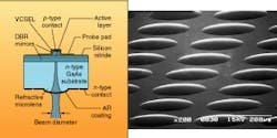
Refractive elements
Near-parabolic refractive microlenses have been fabricated on the substrates of bottom-emitting VCSELs in a process requiring only one lithographic step, report researchers at the University of California (UCSB, Santa Barbara, CA; paper CWF14). The back face of a VCSEL-bearing gallium arsenide (GaAs) wafer is spin-coated with a sacrificial layer of polydimethylglutarimide (PMGI). With Shipley 4210 resist, circles carefully aligned to the front-side VCSEL array elements are patterned onto the PMGI. The surface is next etched with phosphoric acid solution to remove a GaAs layer less than 0.5 µm thick, leaving an array of GaAs cylinders capped with the sacrificial layer of PMGI.
The wafer is placed in an oven at 300°C until the PMGI layer flows into a near-parabolic shape. Surface tension from the GaAs cylinders constrains the flowing resist to the initial diameter of the circles. Chlorine reactive ion etching is then used to remove the resist and define the GaAs lenses. Because of the parabolic shape of the resist, the edges of the GaAs cylinder are preferentially removed, resulting in a near-parabolic lens shape (see Fig. 1).
The lens radius of curvature can be varied by modifying the relative etch rates of GaAs and PMGI and the thickness of the PMGI sacrificial layer. The UCSB scientists have successfully produced elements between 10 and 200 µm in diameter, with radii of curvature ranging from 10 to 1000 µm. They have fabricated an array of 126-µm-focal-length lenses roughly 200 µm in diameter on the back face of a VCSEL-bearing GaAs wafer. Reported output divergence from the VCSEL/lens combination was 1.9°, compared to about 7° for the lensless case.
Diffractive elements
An alternative solution to the same problem involves diffractive optical elements that can both collimate and steer the VCSEL beams. Researchers from Sandia National Laboratories (Albuquerque, NM; paper CWF15) developed the lenses to couple VCSEL output to a receiving array in a vertically stacked multichip module currently under development.
The actual lenses are eight-phase-level binary optical structures, produced by electron beam lithography. A layer of polymethylmethacrylate (PMMA) is spun on to the substrate and exposed by a JEOL JBX-5FE electron beam pattern generator. Material removal from the GaAs substrate is performed by chlorine reactive ion-beam etching. The full fabrication process requires a series of three mask and etch steps.
The Sandia group reported fabrication of diffractive microlenses 80 µm in diameter with 110-µm focal lengths. In addition to on-axis elements, they fabricated off-axis lenses capable of tilting the beam axis by 20° or more (see Fig. 2). Power transmission through a 100-µm hole 850 µm from the lens was 80% for the on-axis elements and 75% for the off-axis case, compared to a value of 20% in the absence of lenses.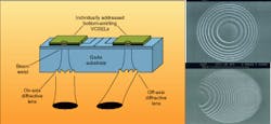
Each method has features to recommend it, whether the minimization of lithographic steps offered by the refractive approach or the beam-steering aspect of the diffractive elements. Rather than being just competing technologies, the two may well become application specific. Either design reduces the number of elements and integration steps required to achieve effective beam coupling, which should make it easier to incorporate VCSELs in optoelectronic systems.
About the Author
Kristin Lewotsky
Associate Editor (1994-1997)
Kristin Lewotsky was an associate editor for Laser Focus World from December 1994 through November 1997.