UV OPTICS: Nanowire grids make high-performance DUV polarizers
With applications in semiconductor lithography and metrology, ultraviolet (UV) and deep-UV (DUV), polarizers are an area of ongoing research. Improving upon temperature-sensitive thin-film polymer polarizers, bulky crystal and cube polarizers, and commercial 150-nm-pitch wire-grid polarizers (WGPs) that operate down to about 450 nm, scientists at NanoOpto (Somerset, NJ) have developed more-robust DUV nanowire-grid polarizers with a 118 nm pitch that operate down to approximately 250 nm.
High-performance WGPs have a high extinction ratio that is influenced by the pitch (center-to-center spacing) of the grid lines, the linewidth, and depth of the grid elements. Beyond the commercial devices with 150 nm pitch, research has produced 100-nm-pitch aluminum-wire grids using a shadowing deposition technique; however, these devices have very low transmittance and extinction ratio at wavelengths below 400 nm.
To improve transmittance and extinction ratio for DUV wavelengths, the NanoOpto scientists used rigorous coupled-wave analysis techniques to simulate nanowire-grid polarizers and their performance parameters. The analysis showed that good extinction ratio and transmittance could be obtained with polarizers having a pitch of 118 nm, a linewidth of approximately 40 nm, and a depth of 200 nm. Because it is difficult to achieve these physical parameters on a large scale (100 mm in diameter) with existing DUV photolithography, electron-beam lithography, and x-ray lithography techniques, the scientists used a process called DUV interference lithography (also called holographic lithography).
A two-beam interference setup with a 110° angle between the two beams was used, with a continuous-wave single-frequency DUV laser at 266 nm (frequency doubled from a 532 nm Nd:YAG laser) as the source. In air, the setup created a 100-mm-diameter grating with an approximately 148 nm pitch. To reduce the pitch to 118 nm, the researchers used a full-wafer immersion technique to immerse the entire wafer in water. This full-wafer immersion technique, which is patented by NanoOpto, reduces the pitch by a factor of n, the index of refraction of the liquid (at 266 nm, n = 1.35 for water).
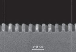
The 100-mm-diameter fused-silica wafer was coated with a 200-nm-thick aluminum film deposited by high-vacuum electron-beam evaporation. A thin layer (approximately 20 nm) of silicon dioxide (SiO2) was then applied on top of the aluminum layer and functioned as a hard mask for the later aluminum-etching step. Finally, a 180 nm layer of photoresist was spin-coated on the wafer surface. The immersion interference-lithography step patterned the photoresist with a 118-nm-pitch grid. After exposure and photoresist development, reactive-ion etching (RIE) was used to etch the grid into the hard-mask SiO2 layer. A final RIE step using chlorine then etched the aluminum to create the nanograting (see figure).
Although some degree of linewidth variation exists, the approximately 40 nm linewidth and 118 nm pitch enable the device to achieve 65% transmittance and a 200:1 extinction ratio at 266 nm. At visible and near-IR wavelengths, transmittance improves to between 85% and 90%, and extinction ratio values of 10,000:1 to 50,000:1 are possible.
“This full-wafer immersion technique will enable us to make uniform and large-size nanowire grids with pitch down to sub-100 nm values,” says Jian Jim Wang, CTO of NanoOpto. “Currently we are working on a 100-nm-pitch version. Continuous reduction of the pitch and the linewidth will further push down the operating wavelength of the nanowire-grid polarizer. We would like to see such thin-film DUV polarizers working down to 193 nm and even 157 nm. Many potential applications require polarizers in the deep-UV regime. Currently, no other cost-effective solution exists.”
REFERENCE
1. J.J. Wang et al., Appl. Phys. Lett. 90, 061104 (2007).
About the Author

Gail Overton
Senior Editor (2004-2020)
Gail has more than 30 years of engineering, marketing, product management, and editorial experience in the photonics and optical communications industry. Before joining the staff at Laser Focus World in 2004, she held many product management and product marketing roles in the fiber-optics industry, most notably at Hughes (El Segundo, CA), GTE Labs (Waltham, MA), Corning (Corning, NY), Photon Kinetics (Beaverton, OR), and Newport Corporation (Irvine, CA). During her marketing career, Gail published articles in WDM Solutions and Sensors magazine and traveled internationally to conduct product and sales training. Gail received her BS degree in physics, with an emphasis in optics, from San Diego State University in San Diego, CA in May 1986.