VCSELs: High-intensity bowtie VCSEL enables near-field applications

With their small spot size and ability to be manufactured using low-cost two-dimensional-array fabrication methods that facilitate simple performance characterization, nanoaperture vertical-cavity surface-emitting lasers (VCSELs) are ideal for such near-field applications as optical recording and single-molecule fluorescence and spectroscopy. Nanoaperture VCSELs with conventional circular or square apertures have poor power-transmission efficiency (when the aperture size is much smaller than the emission wavelength); however, researchers at Stanford University (Stanford, CA) have now developed a bowtie-shaped nanoaperture VCSEL that delivers 188 µW (47 mW/µm2) that is capable of producing up to 150 Gbit/in.2 optical-storage densities.1
Operating at 970 nm, the bowtie VCSEL is composed of 9.5 layers of p-type distributed Bragg reflectors (DBRs), followed by three strain-compensated indium gallium arsenide/gallium arsenide phosphide quantum wells, followed by 38.5 pairs of n-type DBR layers. A half-wavelength-thick silicon dioxide (SiO2) film sits on top of the p-type layers and is capped with a 150 nm gold (Au) coating to improve reflectivity. The SiO2 layer improves the transmission through the nanoaperture etched into the Au layer in three ways. First, the low-refractive-index SiO2 layer reduces the reflection from the nanoaperture at the interface between the Au layer and air. Second, a Fabry-Perot resonance can build up inside the SiO2 layer and beneficially increase the intensity incident onto the nanoaperture. And finally, the SiO2 layer enhances the excitation of surface plasmons at the Au/air interface.
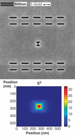
Studies of bowtie antennas, which can serve as near-field probes, reveal that a complementary bowtie-shaped aperture can be designed that optimizes power transmission from the nanoaperture VCSEL. Using a finite-difference time-domain simulation to optimize the design, a bowtie aperture with an outline of 180 × 180 nm and a gap of 30 nm was chosen so that the resonance peak was near the lasing wavelength. The optimization of these parameters reflects the fact that increasing the bowtie outline dimension causes the resonance peak in the transmission spectrum to redshift, while the spectrum blueshifts with increasing gap length. Balancing these two dimensions for the bowtie aperture produces a power-transmission efficiency that is much higher than for conventional square apertures.
Polarization-pinning slits
Because the transmission of light through a bowtie aperture is polarization-dependent, the researchers created 20 slits with sizes of 50 × 280 nm in the Au coating using a focused-ion beam to accompany the bowtie aperture (see figure). These slits have much higher transmission for light polarized perpendicular to the slits than for that polarized parallel to the slits. Hence, the polarization parallel to the slits has lower transmission loss in the VCSEL, pinning the polarization of the VCSEL along the direction parallel to the slits. The power emitted from each slit is two orders of magnitude smaller than that emitted from the bowtie aperture.
Using a 1 cm2 circular silicon detector positioned 4 mm above the bowtie aperture, the researchers recorded a total far-field maximum net power of 188 µW-a power level 16 times higher than that from a 130 nm conventional square aperture that has the same area as the bowtie. And because approximately 10 mW/µm2 is needed for optical recording, the 47 mW/µm2 at a 20 nm vertical distance from the bowtie-aperture VCSEL (contained in a 64 × 66 nm simulated spot size), as well as the estimated 172 mW/µm2 at a 5 nm vertical distance (contained in a 34 × 36 nm simulated spot size), is more than adequate for optical-recording applications.
In addition to the bowtie-shaped aperture, the researchers also experimented with C-shaped and H-shaped apertures, finding significant transmission enhancement over conventional square apertures. “Nanoaperture VCSELs using the bowtie-shaped, C-shaped, or H-shaped apertures can potentially be the key component for the next-generation optical data-storage system with ultrahigh density and data-transfer rate,” says researcher Zhilong Rao. “These high-intensity nanoaperture VCSELs also enable a number of other near-field optical applications such as near-field imaging and analysis and manipulation of molecules.”
REFERENCE
1. Z. Rao et al., Optics Lett.32(14) 1995 (July 15, 2007).
About the Author

Gail Overton
Senior Editor (2004-2020)
Gail has more than 30 years of engineering, marketing, product management, and editorial experience in the photonics and optical communications industry. Before joining the staff at Laser Focus World in 2004, she held many product management and product marketing roles in the fiber-optics industry, most notably at Hughes (El Segundo, CA), GTE Labs (Waltham, MA), Corning (Corning, NY), Photon Kinetics (Beaverton, OR), and Newport Corporation (Irvine, CA). During her marketing career, Gail published articles in WDM Solutions and Sensors magazine and traveled internationally to conduct product and sales training. Gail received her BS degree in physics, with an emphasis in optics, from San Diego State University in San Diego, CA in May 1986.