'Faster, smaller, cheaper' drives laser and O/E product development
As the laser industry moves into its fifth decade, the technology bears little resemblance to what its forefathers—Ted Maiman, Charles Townes, and Arthur Schalow—could have imagined back in the simple ruby-rod days. Who would have thought then that lasers would one day be used to pump one another, transmit data, fabricate semiconductor chips, cut car parts, restore vision, reshape tissue, analyze DNA, and help keep the bad guys at bay?
This industry has often been accused of having too many inventions in search of too few applications. But the last few years have seen a flurry of product development inspired by broad-scale application needs in telecommunications, semiconductor manufacturing, and medicine, which in turn has opened up new market opportunities for these same technologies. In fact, with most of the world's economies bogged down in recession, technology development has taken a front seat in the laser and optoelectronics field. This time, however, much of the R&D is focused on finding new ways to solve old problems and reduce costs in the process.
Telecom drives tunability
With the dragging economy, carriers, systems developers, and components providers alike are taking a step back to rethink and re-engineer many of their products and processes. Much of the emphasis in the past two years has been on meeting the demand for long-haul and ultralong-haul optical networks, but attention has now turned to metro and metro-access networks. And while many of the carriers and systems providers are investigating 40 Gbit/s transmission rates, much of the actual components R&D work is actually focused on improving 10-Gbit/s cost and performance. In fact, there is so much new activity in the 10-Gbit/s arena that many in the industry have revised their timelines for the deployment of 40-Gbit/s networks by at least a year.
"Two general trends in the fiberoptic communication device business at the forefront this past year include a real drive to take cost out of the product and, for the same amount of functionality, make it smaller, less power hungry, and cheaper. The other trend is to develop new components with more functionality," said Fred Leonberger, CTO and senior vice president for JDS/Uniphase (San Jose, CA).
In terms of product development, the important segments in the near term are associated with lighting new channels, not laying or lighting new fibers, according to Tim Day, CTO and vice president of New Focus (San Jose, CA). Thus, transponders, transceivers, interleavers, modulators, and mux/demuxers have become important product areas and will remain so into mid-2002.
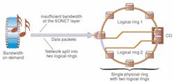
The drive to increase the performance of 10-Gbit/s networks and move beyond point-to-point applications into so-called "mesh" configurations is also pushing the development of new tunable diode lasers—and, according to a growing consensus in the laser community, delaying the potential deployment of 40-Gbit/s networks. Initially these lasers, which will have limited wavelength range in early commercial volumes, will be used as drop-in replacements for existing lasers. Eventually, however, they will offer network managers the ability to customize the lasers to meet the changing needs and traffic patterns of the network (see Fig. 1). Product development here is taking three directions, according to Leonberger, high-power distributed Bragg reflector (DBR) lasers, lasers that are fully tunable over the C-band, and high-power external-cavity diode lasers with broad tunability (see Fig. 1).
"People and companies are working hard on this to enable more flexible networks," he said. "The drivers are to develop a 'universal spare,' where any laser can replace any other, and to be able to remotely set up the laser via the network management system and change wavelengths during its lifetime."
Also driving new product development in the telecom components business is the desire to increase the number of channels and incorporate dynamic gain-equalization capabilities. Whereas 12 to 18 months ago many system vendors were still at 4, 8, and maybe 16 channels, all of the top 15 to 20 vendors are now actively considering 40-channel systems and even multiples of 40, according to John Midgley, president and CEO of Lightwave Microsystems (San Jose, CA). Some vendors are also looking at putting the channels closer together to increase capacity without having to increase data rates, and Leonberger expects to see a lot of commercial activity in this area over the next 18 months.
Amplification technologies are also undergoing some important changes, again in an effort to reduce costs and improve functionality by incorporating more sophisticated control systems. In particular, the development of uncooled 980-nm pump lasers is reducing the number of discrete parts needed and streamlining component design.
"You can now get uncooled pumps that reduce the size and cost of the most expensive part of the amplifier," Leonberger said. "This is a very important trend and a further enabler of next-generation metro networks."
Hand in hand with streamlining design is the push to integrate components, either bit by bit or via a platform configuration—again to improve functionality, reduce manufacturing costs, and facilitate the transition to higher gigabit networks. For example, according to Midgley, most of the major systems vendors are also considering moving away from fiber Bragg gratings toward arrayed waveguide gratings (AWGs). Other emerging integrated devices include variable optical attenuator (VOA) multiplexers, dynamic gain flattering filters, add/drop filters for WDM modules, and power-monitoring modules. Ultimately, we should begin to see hybrid modules with a higher level of functionality and integrated passive and active components, according to Leonberger.
"There are two types of integration: the things we are doing based on waveguides and platform technology where you can add multiple functions, and a macro level of integration where you take individual components and put them together," Midgley said. "But three to five years from now, I think we will see the two merging. If you can build more things onto the platform and integrate the discrete functional parts, you reduce the cost of packaging and improve reliability."
Diode-laser drivers
Not everything in the laser and optoelectronics field is contingent upon telecommunications. But one positive byproduct of the telecom bubble has been its influence on the development of new diode-laser technologies and capabilities, which have in turn opened up new applications for these technologies outside of telecom.
"The whole idea is that semiconductor diode lasers can replace almost all other lasers, except for solid-state lasers providing high peak-pulsed powers," said Dan Botez, professor and director of the Reed Center for Photonics at the University of Wisconsin-Madison.
For example, the push to improve the high-speed capability of local area networks at low cost has prompted several efforts to develop 1.3-μm vertical-cavity surface-emitting lasers (VCSELs) because of their improved manufacturability compared to conventional edge emitters. These lasers also can be designed to emit a radially symmetric beam profile (see Fig. 2). The three primary research approaches involve crystal growth on gallium arsenide (GaAs) substrates because that technology allows the formation of high-quality lattice-matched multilayer mirrors.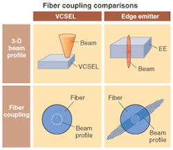
The most promising approach to date is the inclusion of nitrogen in highly strained indium gallium arsenide (InGaAs) quantum wells, according to Botez, as such devices have already demonstrated 10-Gbit/s modulation rates. However, long-term device reliability still remains to be proved. This approach to obtaining 1.3-μm lasing may also become important for medium-distance (metro) telecommunications, since such edge-emitting devices intrinsically have much lower temperature sensitivity of their electro-optical characteristics than that of conventional indium phosphide (InP)-based transmitters. According to Botez, the hope is that the technology can be extended for emission at 1.55 μm, the basic wavelength for long-distance telecommunications.
Industry has also prompted several efforts to develop high-power reliable diode lasers at wavelengths around 0.81-μm and below (down to 0.73 μm), which are important for efficient pumping of solid-state lasers used in many medical as well as printing applications. The solution has proven to be aluminum-free active-region (ALFA) diode lasers. Some companies, including Coherent Semiconductor, already have such products on the market.
Diode lasers that enable the generation of high (0.5 W) CW coherent blue, green, and red powers are also the focus of a number of R&D efforts, according to Botez. Some research groups are experimenting with frequency doubling of red and high-power coherent near-infrared diode lasers to attain relatively high powers of blue and green emission. Fuji already has a frequency-doubled diode-laser product for developing digital film, but Botez sees potential in other arenas as well.
"Commercial blue-emitting diode lasers do exist, but put out relatively modest CW powers (tens of milliwatts)," he said. "However, people in biotechnology (for applications such as flow cytometry) and those interested in laser-projection or laser-display systems need hundreds of milliwatts of blue light. That is why 1-W-range red and/or near-IR coherent powers are needed from diode lasers."
The realization of such diode-laser sources will also allow for the first time the generation of room-temperature CW mid-IR (3 to 5-μm wavelength) coherent-light generation (via frequency upconversion). This will have a revolutionary impact for both noninvasive medical-diagnostics techniques based on laser-absorption spectroscopy (such as breath analysis and body-fluid analysis) as well as for military applications such as IR countermeasures. Botez believes the necessary high-coherent-power near-IR lasers are likely to become practical in the next couple of years.
Silicon processing
Semiconductor manufacturing is also proving to be a fertile incubator for next-generation lasers and applications. Via drilling of high-density interconnects (HDIs) for consumer electronics has become a well-established application for deep-ultraviolet lasers; these days, high-power diode-pumped UV lasers can produce 300 to 500 vias/sec, according to Ed Swenson, senior vice president of technology assessment at ESI (Portland, OR; see Fig. 3).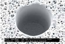
But the never-ending drive to manufacture higher volumes of faster chips that can hold more information is pushing the industry to migrate from ceramic chip packages to silicon chips only slightly larger than the interconnects themselves. This trend is creating a new market for laser-based drilling and scribing of silicon and three-dimensional stacked interconnects, according to Swenson.
"There is great interest in drilling vias and scribing silicon wafers for stacked ICs to interconnect them vertically rather than horizontally," Swenson said. "The whole area of silicon device processing is opening up because when the silicon wafers get thin and you want to cut them to put them in, say, smart cards, or stack them together, they are very brittle. With the laser, you can stack a lot more on the wafer because the laser can go around any shape you want it to." Eventually, deep-UV laser systems will also be used to cut the diode arrays used in making the lasers and diodes used in fiberoptic communications, he added.
These applications are pushing current laser drilling and scribing systems to their limits and prompting companies like ESI to focus on developing the next generation of deep-UV laser systems that have shorter wavelengths, higher repetition rates, and smaller spot sizes. Eventually, Swenson believes ultrafast lasers will become practical for these applications, but he thinks they are still several years away from being ready to work full-time in a class I or class 10 clean room because of reliability and cost issues.
"The challenge is, if you continue to shrink the size of the link and the pitch between the link, we will ultimately have to shift from 1.3 μm to some other wavelength of UV," Swenson said. "Right now we are looking at short-wavelength fourth harmonic generation UV (256 nm)."
Like many of his colleagues, Swenson believes that the diode laser, particularly as a replacement for lamp pumping, has opened up a whole range of applications previously unavailable to lasers. And as the technology continues to improve and become more flexible and affordable, the number of applications for this technology just seems to keep growing.
"The whole movement to diode-pumped lasers is revolutionizing laser technology," Swenson said. "For 25, 30 years, people would only use lasers if they couldn't find another way to solve the problem. But in the last 10 years, it has gone from 'gee, I hate to use lasers' to 'gee, why can't I use a laser?' "
Editor's Note: It is impossible to cover all new technology development in a single article. Future articles will cover emerging technologies in optics, imaging, instrumentation, and displays.
About the Author
Kathy Kincade
Contributing Editor
Kathy Kincade is the founding editor of BioOptics World and a veteran reporter on optical technologies for biomedicine. She also served as the editor-in-chief of DrBicuspid.com, a web portal for dental professionals.