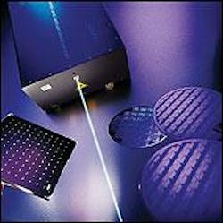
UV laser light reveals killer defects
By Colin Seaton

As IC chipmakers set their sights on moving from 180-nm features to 100 nm and smaller, they are also raising throughput by increasing wafer size from 200 to 300 mm. As feature sizes shrink, so too do the size of "killer" defectslithography errors, voids, and contaminating particles that can cause failures in ICs. This puts pressure on laser manufacturers to help produce leading-edge metrology equipment.
With 180-nm features, manufacturers must be able to locate and identify defects smaller than 125 nm. At 130-nm feature size, the flaws they must detect become smaller than 100 nm.1 As the size of the killer defects shrinks, the sensitivity of the inspection laser has to increase.
One way to increase sensitivity is to produce more power at a given wavelength, thus creating more photons for the light-scattering process to work with. Ultimately, however, the physics of any type of light-scattering technique determines that one must eventually reduce the inspection wavelength as wellthe best solution is to combine shorter wavelengths and higher output powers.
Defect-inspection systems use continuous-wave (cw) lasers to yield a sufficient flux of scattered light and data rates for sensitive detection. As the laser wavelength moves into the ultraviolet, power decreases because of inefficiencies in the harmonic conversion. And while pulsed lasers offer easier harmonic conversion, the data rate requirements of current semiconductor-inspection tools dictate that cw lasers are preferable.
At shorter wavelengths, the diffraction-limited spot size of the laser beam becomes smaller. A smaller spot size covers a smaller wafer area; so again, it becomes important to increase the power to maintain the desired inspection throughput. This requirement becomes even more critical with the move from 200- to 300-mm wafers.
Current inspection systems typically incorporate a 488-nm, air-cooled argon-ion laser to enable the process of light scattering. Unfortunately, laser noise can mask the return signal from the sample under inspection, limiting the sensitivity of the tool. Other drawbacks are the inefficient and inherent bulkiness of the laser. Newer tools based on water-cooled argon-ion lasers emitting at 364 nm provide increased sensitivity. Tools with even higher sensitivity are entering the marketplace. These frequency-double a 514-nm wavelength to achieve 257-nm output.
Newer diode-pumped solid-state (DPSS) lasers offer improvements based on the lasers' smaller size, lower power consumption, and reduced cooling requirements. To date, these lasers have been based on diode-pumping infrared-emitting lasers, such as Nd:YAG and Nd:vanadate, which are converted to the visible (532 nm) by second harmonic generation. A second stage of harmonic generation produces UV output. Starting with a 532-nm DPSS laser, a resonant enhancement cavity uses frequency-doubling to produce a beam at 266 nm, with a cw output power of more than 200 mW. These characteristics make the laser useful for finding even smaller defects.
Recently, a new solid-state technology has emerged. The optically pumped semiconductor laser (OPSL) is based on a semiconductor gain medium tailored to produce the desired 488-nm wavelength. This technology overcomes the limitations of the argon-ion laser in terms of utility costs, thermal characteristics, size, and noise.
Looking forward, IC manufacturers will require cw lasers with wavelengths shorter than 200 nm. Researchers, therefore, are pursuing various methods based on nonlinear combinations of wavelengths. Coherent has reported a cw laser at 198 nm, reached by mixing 244 nm from a frequency-doubled ion laser in a diode-pumped 1064-nm laser cavity with a new crystal called cesium lithium borate.
Colin Seaton
Business Development Manager
Semiconductor and Microelectronics
Coherent (Santa Clara, CA)
[email protected]
REFERENCE
1. Semiconductor Industry Association, International Technology Roadmap for Semiconductors (Austin, TX: International SEMATECH, 1999).