Ultraviolet etches transparent dielectrics
Optical materials such as glasses, ultraviolet (UV)-transmitting oxides like silicon dioxide (SiO2) and sapphire, and fluorides like calcium fluoride (CaF2) and magnesium fluoride are increasingly used in integrated and micro-optics and in biomedical microreactors. These uses require effective and high-grade microstructuring of optical surfaces. Appropriate etching processes rely on mask imaging or beam scanning using either particles or radiation.
While UV radiation is well-suited for the microablation of polymers as well as for the exposure of photoresists in semiconductor lithography, it fails in the treatment of UV-transparent materials. Ultrashort and highly intense laser pulses may be applied to take advantage of nonlinear absorption, but then costly laser systems are required.
A new etching method uses radiation from standard excimer lasers and works even on deep-UV-transparent materials such as CaF2. Its only drawback: the surface to be structured must be in contact with a UV-absorbing liquid during the etching procedure. The pattern to be generated is imaged onto the solid-liquid interface through the UV-transmissive substrate. The patterning speed is an order of magnitude greater than that obtainable in air using the same exposure.
This technique was first proposed a few years ago.1, 2 Now, a research group at the Institut für Oberflächenmodifizierung (Leipzig, Germany) has worked out the details, succeeding in fabricating micro-optical components, some that have three-dimensional geometry.3
The experimental setup consists of a 248-nm-emitting excimer laser, a mask pattern, and a demagnifying objective that images the mask pattern onto the rear side of a substrate that serves as a window of a cell containing the UV-absorbing liquid. Fluids such as pyrene in acetone, tetrachloroethylene, or cyclo-hexane were investigated. Etching rates were studied as a function of the solutions and of the fluences applied. The fabricated patterns were analyzed microscopically and by Rutherford backscattering.
Solvent choice has effects
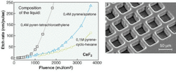
Pyrene, an ultraviolet (UV) absorber, is added to other solvents to enable etching of optical materials at deep-UV wavelengths (left). By themselves, the pure solvents do not absorb UV radiation. There is a considerable difference in etch rate between 0.4-M (1 M = 1 mol/l) pyrene in acetone and 0.4-M pyrene in tetrachloroethylene. In addition, the threshold fluence is reduced from 650 mJ/cm2 for acetone to 180 mJ/cm2 for tetrachloroethylene; the UV absorbing capacity of pyrene in the latter solvent has been enhanced (chemical reactions may contribute to this effect). Rutherford backscattering analysis gave hints to structural alterations of the surface. Using this technique, blind holes can be etched in fused silica that have very clean, steep sides (right).
In one example, the etch rate vs. laser fluence for CaF2 in contact with pyrene varies depending on the solvent (see figure). Quadratic microstructures of 40 × 40-µm size and 25-µm depth in SiO2 have been generated using a fluence of 0.6 J/cm2 and 1500 shots, showing steep walls, a flat bottom, and no debris. Using contour masking, a three-dimensional micro-optical device was fabricated with a microroughness below 10-nm root mean square (rms).
The Leipzig group used the technique to manufacture a sinusoidal optical grating in fused silica with a period of 780 nm and a depth of 180 nm.4 A phase mask yielded the sinusoidal intensity pattern, which was imaged onto the substrate's rear side. Remarkably, roughness was lower when higher fluences were applied.
The researchers have also investigated etching of technical glasses using a xenon fluoride excimer laser emitting at 351 nm.5 Again, solutions of pyrene in either acetone, tetrachloroethylene, or toluene were applied as the absorbers. Glasses such as Pyrex, 7059 (Corning), AF45, D263, and BK7 (Schott) were included, all of which do not show significant linear absorption at 351 nm. As observed in the earlier studies, the etch process can be divided into low- and high-fluence regimes. Almost optical-grade smooth surfaces were obtained that reached, for example, a roughness of 4 nm rms in Corning 7059 at an etch depth of 3.7 µm.
REFERENCES
- S. I. Dolgaev et al., Quant. Elect. 26(1) (1996).
- J. Wang et al., Appl. Phys. A 68(1) (1999).
- R. Böhme et al., Appl. Surf. Sci. 186 (2002).
- K. Zimmer et al., Appl. Phys. A 74 (2002).
- K. Zimmer et al., E-MRS conf. paper (2002).

