Material advances light full-color LED displays
Material advances light full-color LED displays
Manufacturers borrow laser-diode fabrication techniques to create LEDs from various material systems with outputs spanning the spectrum.
David Martin and Vincent C. Forte
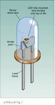
The light-emitting diode (LED) is essentially a p-n junction semiconductor diode that emits monochromatic light when operated in a forward-biased direction. The basic LED structure consists of the die or light-emitting semiconductor material, a lead frame that holds the die, and encapsulation epoxy surrounding and protecting the die (see Fig. 1). The first commercial LEDs were developed in the 1960s by combining three primary elements--gallium, arsenic, and phosphorus (GaAsP)--to produce a 655-nm red-light source. Although the luminous intensity was very low, with brightness levels of approximately 1 to 10 mcd at 20 mA, these early LEDs were still useful for a variety of applications, mainly as indicators.
Following GaAs¥devices, gallium phosphide (GaP) red LEDs were developed that exhibited very high quantum efficiencies (photons emitted per number of charge carriers--that is, current--through the LED). However, Ga¥LEDs played only a minor role in the growth of new applications for two reasons. First, the 700-nm wavelength emission is in a spectral region in which the sensitivity of the human eye, centered about 550-nm green light, is very low. Therefore, this light does not appear very bright to the eye even though device efficiency is high. Second, this high efficiency is only achieved at low currents--as current increases, the quantum efficiency decreases. This effect is a disadvantage to many users such as outdoor message-sign manufacturers who typically multiplex their LEDs at high currents to achieve brightness levels similar to that of continuous dc lam¥operation. As a result, Ga¥red LEDs are used in only a limited number of applications.
Simply red no longer
As LED technology progressed through the 1970s, additional colors and wavelengths became available. The most common materials were Ga¥green and red and GaAs¥orange, yellow, or high-efficiency red, all of which are still used today. More practical applications also began to develop, such as for calculator, digital-watch, and test-equipment displays.
Although the reliability of LEDs has always been superior to that of incandescent, neon, and other lamps, the failure rate of early devices was much higher than that of present-day devices. One reason for the high failure rates was that actual component assembly was primarily manual in nature. Individual operators performed such tasks as mixing and dispensing epoxy and placing the die in position all by hand. Defects such as "epoxy slop" resulted that caused forward-voltage and reverse-voltage leakages or even short circuiting of the p-n junction. In addition, the growth methods at the time, vapor-phase epitaxy and liquid-phase epitaxy, and the materials used were not as refined as they are today. Crystal defects and high numbers of dislocations in the substrate and epitaxial layers resulted in reduced efficiency and shorter device lifetimes.
The 1980s saw the introduction of gallium aluminum arsenide (GaAlAs), which allowed more diverse applications and caused a rapid growth in LED use. The GaAlAs technology provided superior performance over previously available LEDs: brightness was 10 or more times greater due to increased efficiency and multilayer heterojunction-type structures; operating voltages were lower, resulting in total power savings; and the LEDs could also be easily pulsed and multiplexed for use in scrolling variable-message signs (VMSs).
Applications for LEDs broadened into barcode scanners, fiberoptic data-transmission systems, outdoor message signs, and medical equipment, such as blood oximeters. Although major breakthroughs were made, there were still significant drawbacks to using GaAlAs material, which was essentially only available in a red 660-nm wavelength. Yellow, green, and orange exhibited only minor improvement in brightness and efficiency. This lack of improvement was due primarily to the fact that the basic structure of the material remained relatively unchanged and only advances in crystal growth and optical design were made. Also the light output degradation of GaAlAs is more rapid than that with standard technology.
Borrowing laser ideas
To overcome these difficulties, new technology was needed, which led LED designers to turn to laser diodes for solutions. In the late 1980s, laser diodes with visible output began to be commercially produced for applications such as barcode readers, measurement and alignment systems, and optical-data-storage systems. Already involved in visible laser-diode technology, Toshiba (Tokyo, Japan) designers sought to use similar materials and fabrication techniques to produce high-brightness and high-reliability LEDs. This technology resulted in the use of indium gallium aluminum phosphide (InGaAlP) as an LED luminescent material, providing flexibility in the design of output color. By simply adjusting the size of the energy bandgap, green, yellow, orange, and red LEDs all could be produced using the same basic technology.
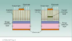
The wafer-level LED design requirements were met by the metal-oxide chemical-vapor-deposition (MOCVD) growth process. Using MOCVD as the growth method, Toshiba was able to produce a device structure that reflected 90% or more of the generated light traveling from the active layer to the substrate back as useful light output (see Fig. 2). This technique allowed an almost twofold increase in the LED luminance over conventional devices. Performance was further improved by introducing a current-blocking layer into the LED structure. Current flow immediately below the wire bonding electrode was not being efficiently used, because the light produced there would not normally have a simple exit path from the LED. The current-blocking layer essentially channels the current through the device away from the light obstructing electrode to achieve better device output efficiency.
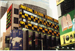
Finally, the light-output degradation over time of InGaAl¥was a significant improvement, even at elevated temperature and humidity. As a result of these developments, two notable application areas represent much of the growth potential for these LEDs in the 1990s. The first is traffic-control devices such as sto¥lights, pedestrian signals, barricade lights, and road hazard signs. The second is VMS, such as one located in New York`s Times Square that displays commodities, news, and other information (see photo on p. 119).
Blue LEDs complete spectrum
Only recently available in production quantities, blue LEDs will result in an entire generation of new applications. Blue LEDs have always been difficult to manufacture, because of their high photon energies (more than 2.5 eV), and apply, because of their relatively low sensitivity to the eye. In addition, the technology necessary to fabricate these LEDs is very different and far less advanced than for now-conventional LED materials. The blue LEDs available today consist of gallium nitride (GaN) and silicon carbide (SiC) with brightness levels in excess of 1000 mcd at 20 mA, for GaN devices. Because blue is one of the primary colors, along with red and green, full-color solid-state LED signs and video displays can eventually become commercially available. Full-color LED signs have already been manufactured, but on a small prototype basis, due to the high cost of blue LEDs. Other applications for blue LEDs include medical diagnostic equipment and photolithography.
It is also possible to produce other wavelengths and colors using the same basic GaN technology and growth processes. For example, a high-brightness green (approximately 500 nm) LED has been developed and is being evaluated for use as a replacement for green bulbs in traffic lights. Other colors including purple are also possible by adjusting material composition.
Projecting further into the future, it has always been a goal for LED manufacturers to replace incandescent lamps with these solid-state counterparts. Although this substitution has been realized in many applications, it is still not practically feasible where a high-intensity white light is required.
With blue LEDs, it is now possible to produce white light by selectively combining the proper amounts of red, green, and blue (RGB) light. Another approach being taken to achieve white-light output is to use a phosphate layer of yttrium aluminum garnet on the surface of a blue LED.
By using quaternary InGaAl¥material, with MOCVD as the growth mechanism, together with efficient delivery of generated light and efficient use of injected current, Toshiba has been able to produce bright, efficient, and reliable LEDs. These devices include red LEDs with typical brightness u¥to 15,000 mcd, orange LEDs at 20,000 mcd, and yellow LEDs having u¥to 23,000-mcd typical brightness. Such technology, together with other novel LED structures commercially available, will ensure wide application of LEDs in traffic-management systems and LED signboards. The new developments in the blue region of the spectrum and for white-light output will ensure increased application of these economical light sources. o
Rolling-display variable-message signs, such as this one in Times Square, New York City, are using InGaAl¥materials for long lifetimes.
FIGURE 1. Typical light-emitting diode (LED) construction was originally accomplished with intensive and error-prone hand assembly.
FIGURE 2. A current-blocking layer within the InGaAl¥LED structure forces the injected current into regions where the light emission is not blocked by the wire-bonding electrode at the to¥of the device.


