According to the Laser Focus World Annual Review and Forecast, material processing is the largest worldwide market for nondiode lasers and will account for laser sales of more than $800 million in 1997, an increase of 25% over 1996 (see Laser Focus World, January 1997, p. 72). Marking, metal working, semiconductor and microelectronic processing, and rapid-prototyping represent just a few of the more-significant laser-based materials-related applications.
The growth of material-processing markets seems likely to continue at impressive rates; as we understand more about the interaction of laser light and materials, the application of all types of lasers to material processing is becoming increasingly widespread. While understanding the processes involved is a key aspect of this growth, equally important to the expanding range of applications is the evolution of laser technology itself. Smaller, more-efficient, and more-cost-effective semiconductor lasers, for example, now compete directly in certain materials-related processes. Meanwhile, imaging systems used for process control are becoming more sophisticated, enabling increased automation and better quality control.
For this year`s European Report, which coincides with Laser 97 in Munich, Germany, we asked our contributing editor in the UK, Bridget Marx, to investigate laser-based material processing in Europe. Her report includes coverage of diode-laser processing--which is a significant part of the Laser 97 program, rapid prototyping--which has evolved from the early days of making plastic models to the fabrication of functional prototypes in various materials, and micromachining--which is growing in importance as technology advances demand smaller and smaller feature sizes.
Inevitably, with a report that covers such an extensive topic, and given the limited space available, there will be aspects of material- processing technology that have been omitted. Fortunately, Laser 97 will afford readers an opportunity to learn more and to actually see some of the systems described in Bridget`s report.
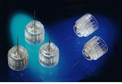
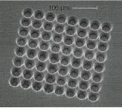
Cover: High-power diode lasers have advantages in welding heterogeneous materials such as metal and plastic components (see p. S5; photo courtesy ILT). Micrograph of three-dimensional array of tiny vertical nozzles illustrates micromachining possibilities for etching silicon with a continuous-wave argon-ion laser emitting at 488 nm (see p. S15; micrograph courtesy of the Technical University of Denmark).
About the Author
Stephen G. Anderson
Director, Industry Development - SPIE
Stephen Anderson is a photonics industry expert with an international background and has been actively involved with lasers and photonics for more than 30 years. As Director, Industry Development at SPIE – The international society for optics and photonics – he is responsible for tracking the photonics industry markets and technology to help define long-term strategy, while also facilitating development of SPIE’s industry activities. Before joining SPIE, Anderson was Associate Publisher and Editor in Chief of Laser Focus World and chaired the Lasers & Photonics Marketplace Seminar. Anderson also co-founded the BioOptics World brand. Anderson holds a chemistry degree from the University of York and an Executive MBA from Golden Gate University.


