Optical-interconnect technology meets standards
Optical-interconnect technology meets standards
New components, applications, and standards are driving parallel-optical-interconnect development, while advances in optoelectronics simultaneously improve dynamic range and reduce power consumption.
Waguih Ishak and Kirk S. Giboney
Several companies have recognized the potential of parallel-optical-interconnect technology for meeting rapidly evolving data-transmission applications such as telecommunications switching or computer networks and clusters. Many of these companies are also pursuing design efforts based on vertical-cavity surface-emitting lasers (VCSELs). The Parallel-Optical Link Organization (POLO), an industrial consortium led by Hewlett-Packard Laboratories (HP; Palo Alto, CA), which just completed its final year in July, was one of these efforts. During its three-year tenure, POLO developed first- and second-generation prototypes, POLO-1 and POLO-2, of a VCSEL-based parallel-optical-interconnect device. This article describes key technical considerations that went into prototype development.
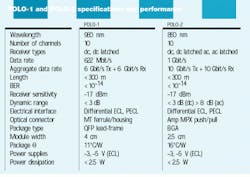
The POLO-1 and POLO-2 ten-channel modules are based on 980- and 850-nm VCSELs, respectively. The respective aggregate data-transmission rates of the two prototypes are 6 Gbit/s and 10 Gbit/s (see table on p. S16). The POLO-2 module is also the first multichip module (MCM) packaged with a ball-grid array (BGA). In addition to device development, the full-design approach taken by the POLO consortium included packaging and interconnection technologies as well as standards. HP partners in the POLO consortium included
AMP (Harrisburg, PA)--a developer of connectors and housings that contributed a latched, push-pull, multichannel, MT-ferrule-based optical connector, as well as a receptacle housing to the POLO design
University of Southern California (USC; Los Angeles, CA)--which provided a link adapter chip that bridges the high-speed signaling of POLO with wider CMOS buses for computer applications
E. I. DuPont de Nemours (Wilmington, DE)--which provided polymer waveguides
SDL Inc. (San Jose, CA)--which developed an edge-emitting laser-based parallel optical link module.
The POLO-1 prototype performs all transmit and receive functions on a single 4 ¥ 4-cm, quad flat-pack (QPC), lead-frame MCM. The electrical interface is differential ECL or PECL. The optical interface is designed for 62.5-µm core multimode fiber and uses (DuPont) Polyguide waveguides. MT ferrules mate in a retainer-type housing.1
Components and assembly
During the development of POLO-1, standards committees chose the 850-nm wavelength for local-area networks. And in response, HP developed 850-nm VCSEL technology for data-communications links that were used in the POLO-2 prototype.2,3
The change in wavelength also necessitated a change in photodetector, because the indium gallium arsenide PIN photodetectors used in POLO-1 do not perform well at 850 nm. Silicon PIN photodetectors are commonly used at this wavelength, but their performance is plagued by low responsivity and by response tails due to absorption in the p region.
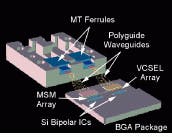
Gallium arsenide (GaAs) metal-semiconductor-metal (MSM) semiconductors offer better responsivity and speed characteristics. In addition, these devices are fabricated in a simple, two-mask process without critical alignments. An aluminum gallium arsenide surface layer provides the passivation to eliminate low frequency gain (see Fig. 2).4
In the POLO-2 prototype, with an 850-nm VCSEL and a 200-µm-square MSM photodetector, rise and falltimes of less than 100 ps and less than 250 ps, respectively, were achieved. Small signal bandwidth was greater than 1.5 GHz, and dc responsivity was about 0.35 A/W. Large photodetector dimensions allowed easy alignment with tolerances of 䕖 µm for the photoreceiver.
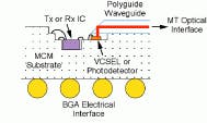
POLO-2 also was designed to be the first optoelectronic integrated MCM with a ball-grid array (see Fig. 3). Higher-density connections through the BGA allowed the overall package dimensions to be reduced to 23.4 mm2. The ball pitch was industry standard at 50 mil, and the multilayer MCM incorporated multiple power and ground planes, extensive bypassing, controlled impedance lines, and thick-film termination resistors in the substrate.
The use of conventional technologies, where possible, in the design of POLO-2 facilitated the use of automated production methods. Polyguide waveguides provided the optical interface, and alignment tolerances of 10 to 20 µm for transmitter waveguides and greater than 50 µm for receiver waveguides would allow fiducial alignment for production assembly. AMP developed the MPX latched push-pull connector as well as POLO-2 housing with MPX-connector receptacles specifically for the POLO project. The overall design of the module and housing isolates the BGA from mechanical forces at the connector (see photo, p. S15).
Performance
Receiver sensitivity in POLO-2 was measured to be about -17 dBm in fiber with a dynamic range of 23.5 dBm at 10-9 bit-error rate (BER). Optical-transmitter output power was uniform across the ten channels, which is important in dc-coupled receivers because of the common threshold for all channels.
For a dc-coupled, unlatched (not retimed) POLO-2 module at 1 Gbit/s using a 27-1 pseudorandom-bit sequence (PRBS), the observed rise- and falltimes were less than 350 ps, and duty-cycle distortion was less than 10%. Jitter on the rising edge of the waveform was caused by the pattern dependence of VCSEL output. The turn-on delay of the VCSELs depends on their history: the longer they are off, the longer the turn-on delay. Biasing the lasers at or just below threshold minimized this effect while maintaining a high extinction ratio. All channels ran error-free during BER measurements to less than 10-14.
Delay through the POLO module was small compared to the optical delay in a fiber of a few meters. For long fiber ribbons, variations in propagation velocities can result in significant interchannel skew.5 Low-skew fiber ribbon can be made simply by assembling the ribbon with consecutive lengths from the same fiber pull, which typically resulted in less than 1-ps/m delay variation. Transmission over 300 m of low-skew ribbon fiber at 1 Gbit/s was also demonstrated with a POLO-2 module.
The ac-coupled receiver offered the advantage of greater channel-to-channel dynamic range at the expense of requiring a dc-balanced ac signal on every channel. The power uniformity was relaxed compared to a dc-coupled receiver. Channel-to-channel dynamic range in POLO-2 was measured to be greater than 8 dB. For comparison, a channel fails in a dc-coupled module when its average power drops 3 dB below the threshold power.
Applications and markets
Immediate applications for parallel-optical links are in high-performance parallel-data systems such as telecommunications switching and computer networks. In telecommunications central switching offices, switch clusters are sometimes connected across distance of hundreds of meters. The entire network must be robust and must be reconfigurable while operating. For the telecommunications industry, parallel-optical interconnects hold out the promise of overcoming the bulk and distance limitations of copper interconnects.
Next-generation computer processors will have clock rates approaching 600 MHz, and even 1-GHz processors are on the drawing board. These clock rates will necessitate tens of gigabytes per second interconnections within computer systems. Parallel-optical interconnects offer a matched, low-latency solution for high-throughput networks of workstations and distributed, multiprocessor systems. As an aid in providing such solutions, USC has developed a link adapter chip that interfaces a POLO module with a workstation bus.6
Recently, HP Laboratories developed VCSEL devices with extremely low threshold currents (below 200 µA) and was able to modulate these devices at 10 Gbit/s. In a few years, packaging technology will probably be advanced enough to allow fabrication of large VCSEL and detector arrays with modulation speeds in the 10-Gbit/s/channel range. With this in mind, it is reasonable to predict interconnect modules using 32 VCSELs with a total aggregate data rate of 300 Gbit/s.
A program has been initiated at HP to commercialize POLO concepts and technologies. And a product-development team is focused on meeting the needs of relevant markets. This program encompasses a family of products, such as appropriate numbers and types of channels that will target classes of applications. A roadmap for addressing market needs has been defined. In February 1996, HP introduced its first commercial VCSEL-based transceiver product and plans to expand this offering into a variety of multichannel optical link modules.2 o
ACKNOWLEDGMENTS
POLO represents efforts of several individuals and organizations. Contributions of the following people are gratefully acknowledged: Kenneth H. Hahn, Joseph Straznicky, Christopher Kocot, Eric G. Wong, Tsu-Yau Chuang, Michael R. Tan, Richard P. Schneider, and David W. Dolfi at Hewlett-Packard Laboratories; Robert E. Wilson, Peter H. Mahowald, Frank Flens, Jeffrey A. Schnur, R. Daniel Rausch, and C. Steven Joiner at Communications Semiconductor Solutions Division, Hewlett-Packard Co; Erwin H. Mueller, Alan E. Plotts, and Dale D. Murray at Optical Interconnection Systems, AMP Incorporated; Joseph E. Marchegiano and Bruce L. Booth at Central Research and Development Laboratories, E. I. Du Pont De NeMours and Company; Barton J. Sano, Bindu Madhaven, Barath Raghavan, and Anthony F. J. Levi at the Department of Electrical Engineering, University of Southern California. POLO is supported by DARPA contract number MDA 972-94-3-0038 and benefits from the guidance of program manager Anis Husain.
REFERENCES
1. K. H. Hahn et al., IEEE Proc. 46th Electron. Component. & Technol. Conf., 301 (May 28-31, 1996).
2. Hewlett-Packard 850-nm Gigabit Ethernet Fiber Optic VCSEL 1X9 Transceiver, HFBR-5305 (1996).
3. K. H. Hahn et al., Electron. Lett. 29, 1482 (August 1993).
4. M. Klingenstein et al., Solid State Electronics 37(2), 333 (1994).
5. S. Siala et al., Electron. Lett. 30, 1784 (Oct. 1994).
6. B. Sano, B. Madhavan, and A. F. J. Levi, Electron. Lett. 32(24), 2262 (Nov. 21, 1996).
FIGURE 1. The complete POLO-2 prototype module included an MPX connector and MT waveguide. Design of module and housing isolated ball grid array from mechanical forces at the connector.
FIGURE 2. Switching from a 980-nm VCSEL in POLO-1 to the 850-nm VCSEL
in POLO-2 required fabrication of a GaAs metal-semiconductor-metal
photodetector (top) to improve responsivity.
FIGURE 3. The ball-grid array (BGA) interface in POLO-2 facilitated higher connection density and a reduction in device dimensions and the use of conventional technologies facilitated automated production methods.


