Light-emitting transistor offers direct megahertz modulation
Researchers at the University of Illinois at Urbana–Champaign (UIUC) have invented a transistor in which the signal output of one of the terminals is IR light. Milton Feng, Nick Holonyak Jr., and Walid Hafez created the light-emitting transistor (LET) and showed that it is capable of switching speeds as fast as 1 MHz.1 Compact, fast-switching devices based on the LET could help more tightly integrate high-speed optical and electrical circuitry for display or communications applications.
In operation, transistors always lose some energy as heat. In some semiconductors other than silicon, losses can be in the form of photons close to or in the visible part of the spectrum. While this phenomenon has been known for decades, development of transistors has focused on maximizing current flow and minimizing losses to heat or light.
Electronics designed to emit light, such as light-emitting diodes (LEDs) or laser diodes, tend to be p-n junctions with only a cathode and anode connection. A bipolar transistor has two junctions and three connections: the base, the emitter, and the collector. "The usual transistor as known and used is a two-port device—an electrical-signal input and an electrical-signal output. In the LET the optical-signal output is a third port," explains Holonyak.
The research
The indium gallium phosphide/gallium arsenide (InGaP/GaAs) heterojunction bipolar transistor produces light from the recombination of holes and electrons in the base layer. Instead of ignoring or minimizing light emission, the researchers tried to optimize the optical output and show that it can be modulated at high speeds.
They used metal-organic chemical-vapor deposition to lay down the layers: first a 350-nm-thick n-doped GaAs collector, then a 60-nm p-doped, compositionally graded InGaAs base, an 80-nm-thick n-doped InGaP emitter, and finally a 100-nm-thick n-doped InGaAs emitter contact cap (see Fig. 1). Etching and depositing contacts creates a working transistor in which a small area of the base layer is uncovered, allowing photons to escape. The entire transistor takes up a 1 × 16-µm space on the chip.
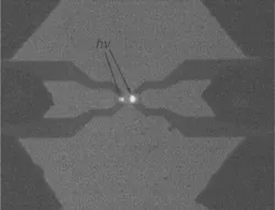
The device's characteristics make recombination (and light emission) occur much faster than in LEDs. The base current keeps the supply of holes in the base high, so when an electron enters the base, recombination occurs rapidly. The 885-nm IR light was emitted from the small portion of the base layer (about 1 × 2 µm) that wasn't obscured by the contact layers of the device (see Fig. 2). The IR light was detected with an avalanche-photodiode setup. The amount of optical output, says Holonyak, was "enough to detect even though only a small fraction of the output is captured."
Current starts to flow in the transistor when the voltage difference between the base and emitter is 1.5 V. When no current was flowing, the researchers saw no light emission from the base. The light-emission intensity from the transistor increased as the base current was increased to 5 mA. When the base current was modulated at speeds as high as 1 MHz, the optical output changed in phase with the base current.
Potential
By varying the band gap, the researchers should, in theory, be able to vary the wavelength of the output photons. Displays that already pair every light-emitter with a transistor could be simplified if multiple-wavelength LETs were developed.
Also, the LET could perhaps be combined with a diode laser, which could be used for high-speed optical buses within computers or integrated multigigahertz communication systems. The 10-Gbit/s laser systems available now use external modulation via lithium niobate or a similar modulator. Lasers with very fast direct modulation, grown on a single wafer, would be smaller, more energy efficient, and possibly cheaper than today's systems.
"The very small active region is akin to that of a vertical-cavity surface-emitting laser (VCSEL)," says LED researcher Russell Dupuis of the Georgia Institute of Technology (Atlanta, GA). "In many ways, VCSEL models fall right into this geometry." In addition to being small, the active region of a VCSEL and the base layer of the LET share high levels of doping and high current densities.
Diode lasers have been modulated for a long time, Dupuis explains, "but the fundamental limit to modulation speed is the radiative lifetime of the electron-hole pairs. That isn't the case for the transistor active region. It's activated by an entirely different process." Electric fields move the charge carriers in transistors, in a process that works much faster than in diode lasers. By developing the (known but previously unwanted) light-emission trait of these transistors, Dupuis says, "They've made a silk purse out of this sow's ear." The UIUC researchers are developing other types of heterojunction bipolar LETs as well.
REFERENCE
- M. Feng et al., Appl. Phys. Lett. 84(1) (Jan. 5, 2004).


