Passive waveguides boost performance and yield
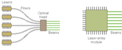
Individually addressable single-mode lasers are used in many industrial and printing applications. In many systems, the light from individually packaged lasers is coupled (usually by fiber) into an optical head (see Fig. 1, left). In a typical module manufacturing process, edge-emitting lasers are chipped into individual devices, mounted on carriers, tested, screened through a burn-in stage, and then packaged individually. The overall manufacturing process is expensive and the system is complex and bulky. Furthermore, the system specification can be constrained because individual lasers are used. In a fiber-coupled system, for example, the spacing between emitters is determined by the accuracy with which the fiber cores can be positioned and the minimum pitch is determined by the fiber diameter. Laser arrays overcome many of these limitations: only one package is required, reducing form factor and cost, and the pitch of the emitters is fixed by lithography (see Fig. 1, right).
For laser arrays to be viable, the manufacturing process must have a high yield and every element must perform within a tight electrical and optical tolerance, with a wavelength range of particular interest being 650 to 1000 nm. This represents a major challenge as the application might require several hundred milliwatts in a single transverse mode from each element. The array also faces the same reliability and yield issues as single lasers but magnified by the fact that there may be up to 100 elements in the array.
Monolithic integration at the chip level is critical in meeting the performance and cost requirements of arrays. The inclusion of passive waveguides adjacent to the facets of the laser cavities not only leads to good electro-optical performance but also relaxes mechanical tolerances. The passive waveguides improve the yield in three ways: the catastrophic-optical-damage (COD) threshold is raised, the cleaving tolerance is relaxed, and the packaging alignment tolerance is relaxed.
Raising the COD threshold
Catastrophic optical damage is the main failure mode of high-power semiconductor lasers operating in the 650- to 1000-nm wavelength range. The semiconductor crystal terminates at the laser facet and the resulting "dangling bonds" give rise to defect states. Electrons and holes recombine via these states, emitting heat instead of light. The temperature rise causes the bandgap to narrow at the facet, leading to strong optical absorption of the laser beam. Therefore, more electrons and holes are created and the facet temperature rises further. The resulting run-away process leads to destruction of the facet. The optical intensity at which this occurs is about 2 × 10⁶ W/cm2; for a mode size of 1 × 3 µm2, this implies an output power of only about 60 mW.
Increasing the single-mode power of semiconductor lasers is a topic of active research. Three approaches are used to raise the COD threshold directly:
- Dielectric coatings. HR/AR coatings are nearly always applied to laser diodes but careful design reduces the electric field at the facet.
- Facet passivation. Materials such as silicon (Si), zinc selenide (ZnSe), and gallium nitride (GaN) reduce the nonradiative recombination rate at the facet (see Laser Focus World, November 2003, p. 69).
- Nonabsorbing mirrors (NAMs). Also known as window lasers—transparent passive waveguides are used in the facet region.
Often a combination of approaches is used and a careful choice of coating material and deposition conditions is always important in achieving reliable high-power operation. The use of NAMs, however, leads to a direct increase in the COD threshold, even of uncoated devices. Having transparent passive waveguides in the facet regions means light is no longer absorbed at the facet, preventing the runaway process responsible for COD.
In addition, the passive waveguide prevents injected carriers diffusing to the facet.
Quantum-well intermixing (QWI) is by far the most common technique for fabricating the passive waveguides. In QWI, point defects are generated at or close to the semiconductor surface; diffusion of these point defects at elevated temperatures results in the intermixing of the wells with the barriers, and a consequent increase in the bandgap energy.1 This creates the passive waveguide at the facet. Quantum-well intermixing is a regrowth-free process and the resulting active/passive interfaces are defect-free and in perfect alignment with the gain section.
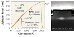
Impurity-induced disordering (IID) using Zn or Si is a widely used QWI process and the first reported NAM laser, as well as more recent reports, used these impurities.2, 3, 4 However, Zn and Si are electrically active impurities, so their use leads to free-carrier absorption losses and current leakage, both of which are undesirable in high-performance NAMs. An alternative approach relies on the fact that point defects are created during sputter deposition of SiO2. The resulting passive waveguide has a low optical propagation loss on the order of a few dB cm-1 (see Fig. 2, left).5 Even for simple devices, under pulsed test conditions the NAM laser has a greater COD level than the standard laser by a factor of 2.6 (see Fig. 2, right).
Cleaving tolerance
The facets of the vast majority of semiconductor lasers are formed by breaking the semiconductor crystal along a cleavage plane. This gives an extremely flat mirror surface but cleaving is a mechanical step whose precision is difficult to control. The typical precision to which cleaving can be carried out is around ±5 µm. Special techniques, such as microcleaving, have a better capability but cannot be used in volume production of high-power lasers. For conventional lasers, the cleave has to be located less than 10 µm from the end of the gain contact. In a laser with passive waveguides the cleaving position only needs to fall somewhere within the passive region. The inclusion of passive waveguides therefore relaxes the cleaving tolerance.
Angular variations in the cleaving direction have an even larger impact, especially for arrays. During conventional photolithography, the laser waveguides are aligned to the crystallographic orientation of the wafer by reference to the major flat. On wafers with high-precision flats, the tolerance with which the major flat is aligned to the crystal plane is about ±0.01°. The lithography system itself will also introduce error, giving a total alignment variation of about ±0.05°. However, the facets are formed by cleaving along the crystal planes, so they are precisely aligned with the crystallographic orientation. The facets are therefore not exactly perpendicular to the laser waveguides.
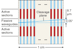
The misorientation is too small to affect the lasing characteristics but introduces a significant uncertainty in the position of the facet relative to the end of the gain section. For a misalignment of ±0.05°, the run-out distance across a 1-cm facet length is as large as ±9 µm (see Fig. 3). Run-out severely impacts the manufacturing yield of laser arrays without passive waveguides; on the other hand, by incorporating suitable lengths of passive waveguides, the yield of arrays can be increased dramatically.
Packaging alignment
Incorporating passive waveguides brings further yield benefits at the packaging stage. Semiconductor lasers are among the most efficient at converting energy to light, with wall-plug efficiencies as high as 50% to 60%. However, the remaining energy is dissipated as heat into a very small volume. A low thermal resistance is therefore required between the active region and a heatsink, so the entire active section must be in close proximity to a subcarrier.
The properties of the laser beam impose further constraints on the alignment. Because of the small dimensions of the waveguide of a semiconductor laser, light is emitted with a large divergence angle. A full-width half-maximum (fwhm) of 30° in the vertical plane is common for a laser operating around 900 nm. Taken together, these constraints mean that the laser must be aligned to the subcarrier with great precision: if the active section overhangs the subcarrier, the laser will fail through overheating, but if the laser is displaced back from the subcarrier edge some light can be obscured.
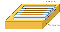
This constraint is particularly serious for an array, when a facet with a length of greater than 1 cm has to be aligned with an angular precision of less than 0.1° to the subcarrier. Again the incorporation of passive waveguides allows these constraints to be relaxed—little heat is generated in the passive sections, so the passive waveguides can safely overhang the subcarrier (see Fig. 4.).
Device design
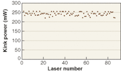
It can be seen from our discussion that the performance and manufacturing yield of laser arrays can be increased substantially by integrating passive waveguides within the laser cavity; indeed such integration is a prerequisite for achieving good yields. The optimum length of passive waveguide sections depends on a number of factors. It must be sufficiently long to meet the laser performance specification; it must accommodate the tolerance in the cleaving position; it must accommodate the tolerance in the cleaving angle (that is, run-out); and it must allow for packaging tolerance. Laser arrays with extremely uniform characteristics have been demonstrated (see Fig. 5).
REFERENCES
- J. H. Marsh, Semicon. Sci. and Tech. 8, 1136 (1993)
- Y. Suzuki, Y. Horikoshi, M. Kobayashi, and H. Okamoto, Electron. Lett. 20, 383 (1984).
- J. K. Lee et al., IEEE Photon. Tech. Lett. 10, 1226 (1998).
- K. Hiramoto, M. Gasawa, T. Kikawa, and S. Tsuji, IEEE J. Select. Topics Quant. Electron., 5, 817 (1999).
- C. L. Walker, A. C. Bryce, J. H. Marsh, IEEE Photon. Tech. Lett. 14(10) 1394 (2002).

