Solid-state UV lasers drill vias effectively

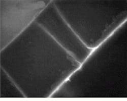
A comparison of the rates of UV-laser ablation of polyimides used in flexible circuit boards has found no significant differences based on laser fluence levels between high-repetition-rate (2-3 kHz) solid-state Nd:YAG lasers operating at 266 or 355 nm and published results based on excimer lasers (see figure). The research, carried out at Electro Scientific Industries Inc. (ESI, Portland, OR), also showed that at high fluences the etch rates obtained using 355-nm lasers are higher than those obtained with lasers operating at 266 nm.
Laser-based micromachining of vias (small holes) in multilayer printed-circuit boards is currently of interest to producers of such circuit boards because the technique creates the vias by a dry photochemical etching process that is both clean and inherently flexible. The laser beam is focused to the diameter appropriate for the hole size required, and size changes are easy to make.
Much of the laser-ablation process has been previously characterized using excimer lasers (see Laser Focus World, Jan. 1996, p. 9), but the relatively recent advent of frequency-shifted, Q-switched solid-state lasers has made available a range of cost-effective UV lasers with potential in this area. Thus, third- and fourth-harmonic Q-switched Nd:YAG lasers provide output at 355 and 266 nm, respectively. The tests at ESI were conducted with solid-state lasers operating at pulse repetition rates between 2 and 3 kHz and average powers of 2?300 mW (at 266 nm) and 2?750 mW (at 355 nm).
According to ESI?s Yunlong Sun, the comparison of laser-ablation rates was conducted to find laser drilling parameters compatible with the many different material components used in circuit boards. Thicker boards, for example, often have 1?5-?m-sized mineral particles added to facilitate handling. The minerals ablate at a much slower rate than the polyimides themselves, which can result in cone-shaped residue with the mineral still remaining at the top. Properly set laser parameters obviate this problem. The researchers, therefore, evaluated UV-laser hole drilling into pure polyimide films with and without mineral particle additives, polyimide films formulated with different polymer chemistry, and polyimide films with binder enhancements.
Test results showed that laser drilling into flexible circuit-board material is readily done using both 266- and 355-nm solid-state lasers and that the ablation rate is higher with the longer UV wavelength at higher laser fluences. The results also showed that, although chemical differences in polyimides can change the laser etch rate, the rates are independent of micron-sized particle additives to the polymers.
About the Author
Stephen G. Anderson
Director, Industry Development - SPIE
Stephen Anderson is a photonics industry expert with an international background and has been actively involved with lasers and photonics for more than 30 years. As Director, Industry Development at SPIE – The international society for optics and photonics – he is responsible for tracking the photonics industry markets and technology to help define long-term strategy, while also facilitating development of SPIE’s industry activities. Before joining SPIE, Anderson was Associate Publisher and Editor in Chief of Laser Focus World and chaired the Lasers & Photonics Marketplace Seminar. Anderson also co-founded the BioOptics World brand. Anderson holds a chemistry degree from the University of York and an Executive MBA from Golden Gate University.