Binary switching node reroutes optical signals
Binary switching node reroutes optical signals
High-speed, monolithic, integrated optoelectronic switches can provide a reconfigurable optical interconnect
for multiprocessor networks.
G. G. Ortiz, A. C. Alduino, and Julian Cheng
Computer systems of the future will feature multiple electronic processors linked to form an interactive network with parallel-processing capabilities. Such systems will have demanding switching requirements. To address these needs, we have developed a compact optoelectronic integrated circuit (OEIC) that provides parallel, high-speed interconnections between electronic processors. The functional integration of optical source, photodetector, and drive electronics within a monolithic device provides a combined optical and optoelectronic switching capability that can convert either electrical or optical input data into both optical and electrical output.
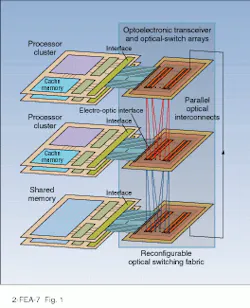
Our approach is based on the dynamic reconfiguration of a multistage, multipath, spatial routing network with a closed-ring geometry (see Fig. 1). Such a system consists of simple optoelectronic switch arrays that provide parallel optical links between nodes and electrical access to an associated electronic processor or shared memory module. Because optoelectronic integration yields extensive yet compact switching matrices, and multiple parallel channels can be routed optically through space, the design offers a large aggregate spatial bandwidth.
A given binary optical routing switch, or node, in the system can be connected to any other node by selecting a path through the closed-ring switching fabric with a small number of intermediate hops. To transmit, receive, and reroute optical data, a node must contain an optical source and photodetector and must be able to convert digital data between various electrical and optical input/output formats. These multifunctional, reconfigurable switching nodes are the backbone of the large arrays that can spatially route many high-speed data channels through dynamically reconfigurable parallel paths.
Using arrays of nodes with associated electronic processors or memory modules, a high-speed optical bus can be built that allows the processors to communicate through parallel interconnections. The optoelectronic transceiver and optical-switch arrays can perform both the photonic and optoelectronic switching functions. Signals are routed by closely spaced, electrically partitioned p-i-n photodiode detectors (PINs) that form a switch with a single input optical port and two output ports. The transmission path can be reconfigured by proper setting of the control voltage.
Switching fabric design
Researchers have previously integrated vertical-cavity self-emitting lasers (VCSELs) with electronic and photonic components to produce optoelectronic devices that function simultaneously as optical transceivers and spatial routing switches.1?5 A single switch consisting of a heterojunction phototransistor integrated with a VCSEL demonstrated 200 Mbit/s operation,3 while an optimized hybrid switch achieved an optical gain of 18.4 However, neither of these switches performed spatial routing. We have improved the performance of the basic single switch by separating the light detection and amplification functions. This allows us to reconcile the conflicting requirements of high current gain, high optical-coupling efficiency, and high speed that limited the performance of previous switches. We have also extended the functionality of the basic switch to include optical routing by closely spacing the PINs to form a switch with a single input and two outputs.
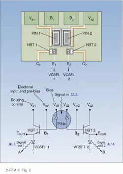
Each node in the reconfigurable fabric consists of a pair of switches, with each switch made up of a VCSEL connected to a heterojunction bipolar transistor (HBT) in an emitter-follower geometry and a PIN connected in parallel to the base-collector junction of the HBT (see Fig. 2). The two PINs are closely spaced and form a single optical input port, while the VCSELs provide two spatially separated optical output ports. When an optical signal is incident upon the PIN pair, two nearly identical photocurrents are generated, each of which is separately amplified by an HBT in the switching circuit.
The amplified current in the circuit can be detected as an electrical current modulation at the collector terminal of the HBT, or it can be detected as a modulated optical output signal generated by the VCSEL. The switches can also each be modulated by an electrical input signal applied at the base terminal of the HBT. Each node can thus act as an optical receiver (optical input, electrical output), transmitter (electrical input, optical output), or routing switch (one optical input, one or more optical outputs) with a fan-out of two.
Device specifications
The HBT has an emitter-up configuration; the lower base-collector junction layers are used to define the PIN (see Fig. 3). The PIN features a responsivity of approximately 0.22 A/W at 850 nm, with a 3-dB bandwidth of 700 MHz. The HBTs have a differential current gain of 100 at a collector current density of 15 kA/cm2; the 3-dB modulation bandwidth for the device is 550 MHz. The 16-?m-diameter VCSELs have a high slope efficiency of roughly 35%, producing 1 mW of optical output at a current of 12 mA and an operating voltage of 2.5 V. Each switch is prebiased near the VCSEL lasing threshold with a dc base current; this minimizes the turn-on delay and reduces the optical power required for switching. The devices demonstrate the conversion of high-frequency electrical input data into large-amplitude optical output data at a data rate of 400 Mbit/s (see Fig. 4); all-optical switching can be performed at the same rate.
Optical input pulses couple equally into the PIN pair of a switching node, producing 40 ?A of modulated photocurrent in each PIN. This current is amplified by the HBT to produce an emitter current that modulates the VCSEL from just below threshold to an optical output level of about 1 mW.
To demonstrate the optical routing and fan-out capabilities of the binary switch, a 500-Mbit/s optical input signal is coupled into the prebiased switching node as described above. When a bias voltage is applied to the collector of each PIN/HBT/VCSEL circuit, the amplified photocurrents produced by the optical-input signal are routed to each of the two optical-output ports, modulating each VCSEL at a data rate of 500 Mbit/s and producing a fan-out of two (see Fig. 5). If only one of the circuits is biased, the data are routed to the corresponding output port.
To cascade these switches in a multistage routing network, each node must provide sufficient optical gain to compensate for losses incurred during transmission. The differential gain for each stage is proportional to the optical coupling efficiency (approximately 36%), the PIN efficiency (approximately 45%), the current gain (approximately 100), and the slope efficiency of the VCSEL (approximately 35%). The maximum optical gain achieved with these switches is 7.5 dB, which is sufficient to allow the cascaded operation of several switch stages.
The new high-speed, integrated optoelectronic switch based on VCSEL and HBT technology can be used to implement a reconfigurable optical-interconnect architecture for multiprocessor networks. Present devices can operate at 500 Mbit/s; future optimization of device design and processing should permit HBT/VCSEL operation at data rates above 1 Gbit/s. n
ACKNOWLEDGMENT
We gratefully acknowledge the contributions of C. Hains, B. Lu, and Y. C. Lu of the University of New Mexico, also R. P. Schneider, M. J. Hafich, J. Klem, and J.C. Zolper of Sandia National Laboratories, Albuquerque, NM.
REFERENCES
1. P. Zhou et al., IEEE Phot. Tech. Lett. 5, 1035 (1993).
2. Y. J. Yang et al., Appl. Phys. Lett. 62, 600 (1993).
3. Y. C. Lu et al., Electron. Lett. 31, 579 (1995).
4. Bo Lu et al., IEEE Phot. Tech. Lett. 6, 222 (1994).
5. W. K. Chan et al., Appl. Phys. Lett. 58, 2342 (1991).
FIGURE 1. A parallel, reconfigurable multiprocessor optical-interconnect network permits data transfer between processors while allowing access to shared resources, such as memory.
FIGURE 2. Binary interconnect switching node (top) consists of two switches, each composed of a vertical-cavity surface-emitting laser source (VCSEL), a p-i-n photodiode detector (PIN), and a heterojunction bipolar transistor (HBT) amplifier. Diagram of node (bottom) shows how routing control voltage applied to the appropriate HBT sends a signal to the proper output port.
FIGURE 3. In a monolithic switch, an amplifier, photodetector, and source are integrated on a single chip. Arrays of these devices may form a simple,
compact, and highly versatile switching fabric.
FIGURE 4. Optical output of single PIN/HBT/VCSEL switch modulated at 400 Mbit/s by an electrical input signal (left) and an optical input signal (right) shows the fidelity of the device. The length of the transmission lines used in the experimental set-up causes the time delay between the input pulse train and the output pulse train.
FIGURE 5. Binary optical switching node can route a single input signal to two separate
output ports.


