Diode lasers light up disks, communications, and printers
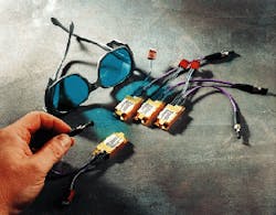
A decade after its invention, and a generation ago, lasers were still something of a novel high-technology gadget looking for applications and markets, seeming more a part of the science-fiction world of death rays than the everyday world of home, store, and factory. Today, lasers are at the heart of the two fastest-growing industries: computers and telecommunications. Laser light carries millions of phone conversations and most of the data traffic on the Internet. Tiny semiconductor lasers read the data stored on CD-ROMs, increasingly vital as a large-scale storage medium for computers as well as the dominant medium for audio recordings. Other lasers are used in the high-quality printers that have revolutionized computer-based desk-top publishing (see photo at top of this page).
What has made this transformation possible is the diode laser, a semiconductor-based laser that can take advantage of the mass-production techniques of the microelectronics industry and of very low per-unit costs of the semiconductor industry. In this first part of Laser Focus World’s new Back to Basics series on lasers and applications, we describe the overall applications, basic operation, materials, structure, and fabrication of diode lasers. In future articles in the series we’ll focus on long- and short-wavelength diodes, high-power diodes, and diode arrays. Later in the year, we’ll review other types of lasers: ion, excimer, solid-state, carbon dioxide, tunable, diode-pumped, and ultrafast lasers.
A light-emitting diode with mirrors
All diode lasers are based on light-emitting diodes (LEDs). As with the photodiode, the underlying structure is a p-n junction—the only difference is the direction of the applied voltage or bias. The p-n junctions consist of a semiconductor layer (silicon in most photodiodes) doped with atoms carrying extra valence electrons (n-type semiconductors) under a layer doped with atoms carrying one valence electron less than silicon (p-type semiconductor). Charge migration creates a depletion region with an electric field directed toward the p region, allowing current to flow in only one direction. In a photodiode, a reverse bias potential is applied across the diode, preventing current from flowing in the absence of light. With exposure to light, electron-hole pairs are created, generating a current.
In an LED, the process is exactly reverse. A positive bias is applied, causing current to flow. As the electrons form the n-type semiconductor flow into the p-type semiconductor, they combine with the holes, releasing energy in the form of light. Because the junctions will absorb light at the same frequency they emit it, the junction must be designed so that the emission occurs near the surface, minimizing reabsorption. Nonetheless, the efficiency of LEDs is fairly low, generally less than 10%, and, as in incandescent and fluorescent light, the emission is emitted equally in all directions.
Diode lasers differ in that light is generated by stimulated rather than spontaneous emission, with the result that the generation efficiency is much higher. To produce stimulated emission, the energy from electrons dropping from the conduction band must be efficiently transferred to the generated photons, because if any significant amount of energy is lost as heat, the resulting photons will have too little energy to stimulate emission from another electron. This limits the materials for diode lasers to those with direct bandgaps, such as gallium arsenide (GaAs), in which the electrons lose energy without momentum being transferred to the lattice. In an indirect bandgap structure, as in silicon, transfer of momentum causes the electron to lose energy in the form of heat, and such materials are unsuitable for diode lasers.
A second difference between diode lasers and LEDs is that lasers require a higher current. Below the threshold current, self-absorption of the emitted light creates too small a population of excited states to sustain laser amplification: a photon is more likely to be absorbed forming a electron-hole pair than it is to stimulate emission from an excited state. With higher current, the excited states become more populated than the relaxed states—the condition known as a population inversion. Laser amplification now occurs because each photon on average produces more than one stimulated photon before leaving the laser or being absorbed. Once this laser amplification occurs, the device’s quantum efficiency in converting additional electrical energy into light jumps to values much higher than those for LEDs. Quantum efficiencies as high as 78% and overall device efficiencies as high as 43% can be achieved in diode lasers.
Laser action requires that emitted light be confined and reflected back and forth to form a directed beam. Typically, diode lasers use the same structure as LEDs, with the active area being confined on the top and bottom by layers with different refractive indexes. The cleaved face at the emitting end acts as a partially reflective mirror, while the other end is generally coated with a reflective coating to produce a fully reflective mirror.
Small, fast, and inexpensive
The small size and low cost of diode lasers makes then suited to a number of key applications. Current injection gives them the ability to be rapidly modulated, and their high efficiency has long made them the workhorse of optical communications. Coherent laser light in the wavelength range around 1510 nm can in theory carry tens of terabits per second over optical fibers. A second major application is in reading optical-disk memories in computers and audio systems. Here, the very small size of diode lasers and their ability to be moved rapidly from track to track makes them ideal for this purpose. The main thrust of development in these applications is to move toward shorter and shorter wavelengths to further increase memory densities, as shorter wavelengths of laser light can be focused to smaller spot sizes.
While diode lasers are used for reading data into a computer, they are even more common in producing output onto paper. Laser printers use diode lasers to scan images onto photoconductive material; in this application their low cost and high reliability are advantageous. These same basic advantages have led to diode-laser use in a variety of sensors, for example, in the laser gyroscopes that are carried on nearly all modern aircraft. In addition, high-power diodes are used in material-processing applications such as plastic cutting and for medical tasks such as photocoagulation in eye surgery.
Diode-laser materials
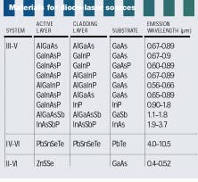
The output frequency (or wavelength) of operation of a diode laser depends on the bandgap of the material used to form the laser structure. Ternary and quaternary compounds allow the bandgap to be changed, depending on the composition of the compound, so these material systems are commonly used (see table). For wavelengths shorter than 1 µm, gallium aluminum arsenide (GaAlAs) grown on a GaAs substrate was among the first compounds used. Another common choice is gallium indium arsenic phosphide (GaInAsP) on GaAs. For longer wavelengths—in the range from 1 to 1.67 µm—GaInAsP can be grown on InP substrate, or AlGaInAs can be grown on the same substrate.Because GaInAsP/InP diodes require thermoelectric coolers, there has been considerable interest in developing new materials that operate at room temperature over the same wavelength range. Last year, researchers at the Hitachi Central Research Laboratory (Tokyo, Japan) reported that indium gallium arsenic nitride (InGaAsN) grown on GaAs substrate can achieve room-temperature operation for wavelengths at least up to 1.3 µm and possibly beyond. For still longer wavelengths (above 2 µm), lead-based compounds can be used. A typical material is lead antimony selenium telluride (PbSnSeTe) grown on a PbTe substrate. Other material systems for infrared operation include indium gallium arsenic antimonide (InGaAsSb) and related compounds grown on either InAs or GaSb substrates (see Laser Focus World, Mar. 1996, p. 77).
In all these materials, lattice flaws must be avoided, which means that all the materials in a laser must have nearly identical lattice spacing. In fact, the match between layers and the substrate must be closer than 0.1%. However, the development of strained-layer technology has allowed the mismatch to increase to 1%, making possible a wider range of materials and wavelengths. A strained layer is a very thin layer, only a few nanometers thick, between two different lattices, which takes up the strain of the mismatch without producing flaws.
Laser structures
The most common structure for diode lasers is the simple stripe edge-emitting type. In this design, the active area, the junction, is a narrow stripe, and light is funneled by internal reflection to the edge. The active layers are surrounded on both sides by different semiconductor materials, not just differently doped material, making what is known as a double heterojunction. Because these materials have different refractive indexes, the active layer acts as a waveguide, directing the light out to the edge (see Fig. 1). In addition, if the doping materials have different bandgaps, as is generally the case, light being refracted through them is not absorbed, cutting self-absorption.The active area is also confined on top and bottom by layers with different refractive indexes. Cleaving the faces at the emitting end creates a partially reflecting mirror, while coating the other end with a reflective coating produces a fully reflective mirror. These mirror surfaces define the laser cavity.
Confinement of the active layers from the side is generally accomplished by either gain- or index-guiding. Index-guiding simply surrounds the active layers on the sides as well as above and below with material with a different index of refraction, while gain-guiding confines the current to a stripe by blocking off the rest of the device with insulating layers. Index-guided stripes can be made as narrow as 1 µm, leading to nearly all the light traveling in the same direction (although diffraction limitations broaden the output beam). Overall, a diode laser is typically about 300 µm in length by 100 µm wide, with active layers of around 2 µm in thickness.
For higher powers and tighter beams, multiple stripes can be arranged into a diode-laser array. In these devices, active layers alternate with inactive areas at a typical spacing of about 10 µm. In more complex ar rays, more than one layer is used, making a two-dimensional array. Such arrays can achieve continuous powers greater than 10 W, and their greater overall width can reduce diffraction effects, generating a narrow beam. This performance is important, especially in fiberoptic applications.
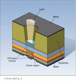
It is not essential that a diode laser be edge-emitting. A newer structure is a vertical-cavity surface-emitting laser (VCSEL). In this design, the active layer is sandwiched below partially reflecting layers and above totally reflective ones (see Fig. 2). Each laser region is exceedingly small, only a few micrometers across, and millions can be placed onto a single chip. Their compactness and low threshold current makes them suitable for optical interconnects and optical computing.Making the diode
Diode lasers are manufactured using the same basic techniques of semiconductor microelectronics. First, layers of material are laid down by epitaxy, then through photolithography patterns are created in resist layers, and finally the exposed parts of the resist are etched away. Often more than one such cycle is need to create a finished diode laser.
Epitaxial growth can be accomplished in a number of ways. In liquid-phase epitaxy, a crystalline layer of material is grown from a saturated liquid solution. This process takes place in a high-purity carbon boat, which contains the substrate in the lower part and a series of bins with melted materials in each bin. For example, one bin might hold gallium, another aluminum, and another gallium arsenide. The substrate is placed in contact with each bin in turn, the temperature is reduced, and an exact thickness of material is crystallized.
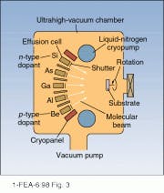
In vapor-phase epitaxy, the material to be deposited is transported as part of a gaseous compound, a halogen such as gallium chloride (GaCl3), or an organometallic compound, such as trimethyl gallium [(CH3)3Ga]. When the vapor touches the substrate, it reacts, depositing the material to grow the crystal. Finally, in molecular-beam epitaxy, the substrate is placed in a high vacuum and bombarded with a beam consisting of the material to be deposited (see Fig. 3). Very thin layers can be grown in this manner, with interfaces thinner than a single atomic layer.The next step is photolithography. Typically, UV light is used to illuminate a mask carrying the pattern desired, which is projected onto the wafer at a demagnification of five or ten times. For even higher-resolution work, x-rays can be used, or, without a mask, electron or ion beams can be directed onto the areas selected. The photoresist material is designed so that exposure to light or other radiation changes it chemically to a form that is soluble in the etching chemical.
In the final stage, an acid is applied to etch away the undesired area. Where the photoresist has been exposed, the etchant removes the layer and the material below as well, while in the other areas, the resist protects the material below it. However, isotropic etching tends to undercut these resist caps, so anisotropic etching, in which the etching rate depends on the lattice direction, is generally used. Dry etching by physical sputtering of material is also sometimes used.
In some devices, gratings are applied to stabilize and/or control the output wavelength. In this fabrication step, holographic interference patterns are generated with lasers, obviating the use of masks and generating high accuracy gratings. Final steps in the fabrication process include packaging and, in some cases, attaching fiber "pigtails" to allow flexibility in the direction of laser output. Manufacturers strive to improve the diode-laser fabrication process to increase yield and further reduce costs, thereby assuring a continued growth of diode-laser applications.
FURTHER READING
Y. Suematsu, ed., Handbook of Semiconductor Lasers and Photonic Integrated Circuits, Chapman and Hill, London (1995).
About the Author
Eric J. Lerner
Contributing Editor, Laser Focus World
Eric J. Lerner is a contributing editor for Laser Focus World.


