Diode lasers offer efficiency and reliability
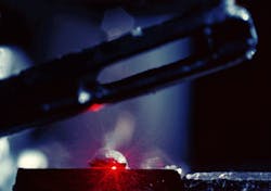
The realm of high-power, industrial lasers that weld and cut used to be the exclusive preserve of gas lasers, which, although easily scaleable, are bulky and inefficient. Now, however, compact and efficient high-power solid-state lasers are expanding rapidly into this area, and the key to that expansion is the use of diode lasers for pumping (see photo at top of this page). At the same time, diode lasers themselves are settling into a large number of high- and medium-power applications, making them one of the industry’s fastest-growing sectors. This growth can only accelerate as long-standing reliability problems, a plague of high-power diode lasers, are overcome with new technologies and materials, especially the use of aluminum-free active regions that resist defect formation.
Why high-power diodes?
In gas lasers, such as those using carbon dioxide, which have long been used as powerful continuous-wave sources, efficiencies are typically low, reaching no more than 20%. Potentially, Nd:YAG solid-state lasers are far more efficient for converting optical pumping energy into laser light. But the traditional method of pumping such lasers is by flashlamps, which produce a wide range of frequencies, while only a narrow range is actually used to pump the laser atoms into an inverted energy distribution. The result is an overall efficiency of around 1%.
The very low efficiency of older high-power lasers, in turn, means that energy sources must be large and cooling requirements great, making such lasers bulky. In general, mobility is achieved by funneling the light from a stationary laser through a movable set of mirrors in an articulator arm, but of course such solutions still severely limit mobility and eliminate portability.
In contrast, diode-pumped solid-state lasers (DPSSLs) can have high overall efficiency, because the diode lasers are themselves highly efficient, and they can pump laser energy directly into the 0.8-0.87-µm band needed. Thus, overall efficiencies of DPSSLs are at least ten times higher than for flashlamp-pumped lasers; so high-power industrial lasers can be made compact and truly portable. The inherent advantages of Nd:YAG lasers are all retained—very high beam quality, nearly diffraction-limited beam divergence, high beam pointing and amplitude stability, high peak power, and repetitive pulsed-mode operation.
High-power diode lasers (generally considered to be those with more than 100-mW output) have a variety of other uses. Broadly speaking, such lasers can be either incoherent or coherent, with the coherent type requiring considerably more-complex structures. Incoherent lasers, in addition to being used for pumping, can provide medium-beam-quality sources with about 40 times diffraction-limited divergence for material processing, with outputs ranging up to several watts. Coherent high-power diode lasers are used primarily for frequency conversion for blue or green sources and for free-space communications—for example, with satellites.
Solving the reliability problems
The power of a diode laser depends directly on its spot size--the size of the active region that is doing the lasing. High-power diode lasers typically have spot sizes in the range of 100 µm. But with high power comes accelerated aging and shorter lifetimes. For pump lasers using aluminum gallium arsenide/gallium arsenide (AlGaAs/GaAs) to produce wavelengths up to 0.84 µm, dark-line defects, which sap the output power, are a leading cause of aging and failure. In addition, surface recombination of holes and electrons release heat that can deteriorate front facets.
There are several approaches to solving this basic reliability problem, but one of the most actively pursued at this time is aluminum-free systems, such as indium gallium arsenide phosphide/ gallium arsenide (InGaAsP/GaAs). These systems have considerable advantages. First of all, dark-line defects spread far more slowly through them than through aluminum-containing systems. "The indium atoms are big atoms," explains Dan Botez of the University of Wisconsin-Madison, "and they serve to harden the lattice, making it difficult for line defects to propagate past them." In addition, the surface-recombination velocity is nearly a hundred times smaller than with aluminum compounds, leading to a much smaller increase in facet temperature with drive current. Finally, reliable indium-based diodes can be grown on silicon substrates, opening the way for very fast wafer-to-wafer interconnects.
Unfortunately, aluminum-free compounds introduce other problems, which are just now yielding to researcher ideas. InGaAsP/GaAs structures have small bandgaps between conduction and valance bands, resulting in massive leakage of current carriers. This in turn leads to low internal efficiency, high threshold-current density, and low threshold-current characteristic temperature.
One solution is to restrict the aluminum-free compounds to the active regions and go back to high-bandgap aluminum compounds, such as AlGaAs, for cladding. This blocks carrier leakage, improving efficiency. In a related design by Botez and his group, InGaAlP, which also has a high bandgap, is used for cladding and decreases the threshold-current density (see Fig. 1). With this method, power output of 4.7 W was achieved with 220-A/cm2 threshold-current density and a 160 K characteristic temperature.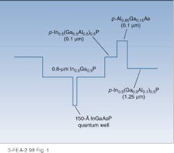
Improving aluminum-device reliability
Another approach to high-power diode-laser reliability is to simply reduce the factors that lead to failure in AlGaAs quantum-well lasers. The biggest cause of such failures is the growth of dark-line defects—lattice dislocations that typically start at the sidewall of a laser chip and propagate inward to the emission region. Generally, when the dark-line defect reaches the emission regions, it spreads out into a network of defects, setting off nonradiative recombination of carriers, liberating heat and sapping energy.
Studies performed at the Polaroid Corp. Division of Laser Diode Manufacturing and Development (Norwalk, MA) showed that most dark-line defects result from defects induced by the mechanical process of chipping or sawing apart adjacent chips. Energy from nonradiative recombination induced at the site of the defect then couples to the lattice, causing the dislocation to climb up through lattice. In some way (still a matter of debate among researchers), the recombination energy causes atoms adjacent to the defect to vibrate sufficiently that they move out of place, creating a new dislocation and renewing the process.
To reduce dark-line-defect formation, the Polaroid group has proposed that the defects created by mechanical stress be isolated from the recombining carriers that can cause the defects to grow into a line. One way of doing this is to etch a trench in the chip all the way down to the substrate level through the regions where the chips will be separated from each other. Only the substrate will then be sawed apart and mechanically damaged. Because the defects will then be farther from the p-n junction, the core of the laser, than the minority carriers` diffusion length, recombination cannot occur at the defect site and the defects cannot grow.
An alternative method would be to introduce a nonconducting region at the edge of each chip to again isolate the mechanical damage from the carriers. Because the carriers could not enter the nonconducting region, defects could not grow through it. To be effective, such techniques would also have to include precautions during manufacture to ensure that defects are not introduced into the bulk of the chip during epitaxial growth. This involves such well-known steps as the use of low-dislocation density substrates and limitation of handling and thermal stresses.
Slowing aging process
Implementing approaches to slow aging requires the ability to monitor such aging, preferably nondestructively. One new way of doing this, developed at the Max Born Institute for Nonlinear Optics (Berlin, Germany), is with near-field photocurrent spectroscopy, which provides extremely high resolution in detecting microscopic defects. Here, light is transmitted through a 50-nm aperture as a probe is moved across the surface of the laser chip at a distance of 5 nm. (Light can penetrate through extremely tiny apertures so long as the probe is kept very close to the surface--that is within the near field. At a greater distance relative to the aperture diameter, light transmission drops rapidly to the vanishing point unless the aperture is larger than a wavelength of light).
As the probe moves, the photocurrent induced across the p-n junction is monitored. By varying the excitation wavelength of the probe photons, a spectrum can be obtained at each point. The changes in defect density induced by aging are clearly detected by this method, and it thus allows continuous monitoring of the aging in each portion of a given chip (see Fig. 2).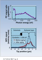
While much of the attention given to high-power diode lasers has been concentrated on their use for pumping in the 0.8-µm range, there is considerable interest in long-wavelength high-power diode lasers for medical applications, eye-safe rangefinding and illumination, and, of course, free-space communications. For example, researchers at SDL Inc. (San Jose CA) and Sarnoff Corp. (Princeton, NJ) have used InGaAsP with a strained multiple-quantum-well structure to achieve 3 W of emission at 1.58 µm and 5.2 W of emission at 1.43 µm, respectively. With bar lasers integrating several active regions, outputs of at least 30 W are anticipated, enough for most applications.
FURTHER READING
G. Holleman et al., SPIE Vol. 2772, p. 2 (July 1994).
F. P. Dabkowski et al., SPIE Vol. 2886, p. 6 (Aug. 1996).
J. K. Wade et al., Appl. Phys. Lett.70(2), 149 (Jan. 1997).
A. Richter et al., Appl. Phys. Lett. 69(26), p. 1981 (Dec. 1996).
About the Author
Eric J. Lerner
Contributing Editor, Laser Focus World
Eric J. Lerner is a contributing editor for Laser Focus World.