SOLID-STATE LASERS: TEM00 CW green laser source is a powerful tool
Thin-disk technology, along with efficient frequency doubling, gives rise to a 50 W CW green laser whose high beam quality is perfect for micromaterials processing.
GÜNTER HUMMELT
High-power visible-light-emitting lasers with near-ideal beam quality have applications in materials processing, including in the microelectronics industry. For these uses, we have developed a true continuous-wave (CW) laser based on thin-disk-laser technology that emits more than 50 W optical power at 515 nm with a TEM00 beam profile (M² less than 1.1). Compared to conventional designs, this is a breakthrough in CW green high power; previously, less than half this output power was available commercially.
Development of this laser is part of the European collaboration project Joitec, sponsored by the European Union and consisting of companies from several European countries (see www.joitec.com). In this particular project, the laser will be used to develop microwelding technologies to replace conventional lead-free soldering techniques.
In addition to lead-free microwelding, the frequency-doubled thin-disk laser will be useful in other areas of micromaterials processing, including the direct welding of nonferrous or noble metals and the micromachining and annealing of silicon and other semiconductors.
Thin-disk versus conventional lasers
One of the recent developments in diode-pumped solid-state laser technology was the invention of the thin-disk laser. Researchers at the University of Stuttgart (Stuttgart, Germany) invented and developed this concept in the 1990s. In this type of laser, the active laser crystal has the shape of a thin disk. Because of its excellent heat management, this technology overcomes the limitations of conventional slab or rod laser designs.
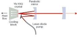
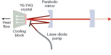
The thin disk is attached to an actively cooled heat sink (see Fig. 1). The pump power from the diode lasers is collimated and directed toward a parabolic mirror. From there, the pump beam passes through the thin disk, gets reflected on the back side of the disk, and travels back to the parabolic mirror, is again reflected to the thin disk, and so on. The geometry of this mirror and additional beam-steering prisms allows the beam to pass several times through the thin disk.
This method of pumping a solid-state laser is known as front-face pumping. The disk is very thin (approximately 150 µm) and the distance from the pump spot to the coolant is therefore short, which results in an excellent heat flow collinear to the optical axis of the laser. Practically no thermal lensing occurs. A TEM00 mode profile at high power levels is easy to achieve and can be maintained over a wide dynamic range.
So far, medium-level green CW power with good beam quality has been achieved in frequency-doubled Nd:YVO4 (vanadate) lasers. In these conventional side- or end-pumped designs, the distance between the beam waist of the pump power superimposed with the lasing beam to the coolant is much longer. The heat flow is perpendicular to the optical axis. This limits the attainable power levels if a perfect Gaussian intensity profile is required. To date, no more than 20 W output power has been commercially available with side- or end-pumped designs.
Most commercially available thin-disk lasers use ytterbium-doped YAG (Yb:YAG) as active material (1030 nm fundamental wavelength, 515 nm with frequency doubling). This crystal has ideal properties for generating high power levels with a good beam profile. The wide absorption peak of Yb:YAG around 940 nm facilitates efficient pumping. Diode-pump modules operating at 940 nm have typical lifetimes of more than 40,000 hours. This is a solid foundation for low cost of ownership and long-term reliability in industrial applications.
Frequency doubling
The ability to generate very high CW power with a perfect Gaussian intensity profile is a central characteristic of efficient frequency doubling. To achieve the required power density for frequency doubling, we use a double-Z resonator that provides a beam waist within which an LBO (lithium triborate) crystal is positioned. This type of crystal, which combines excellent mechanical and optical properties with high doubling efficiency, is widely used for frequency doubling.
Noncritical phase matching is obtained with temperature tuning via an oven-an approach that maintains the beam properties of the fundamental wavelength so that the generated second harmonic has a high-quality TEM00 beam profile with linear polarization.
The design of the oven is critical. The sensitivity of the temperature control is on the order of 0.01°C with a low time constant. We use a design with forced cooling to avoid heat dissipation within the laser head and achieve the short time constant needed for precise temperature control under changing load conditions.
The main hurdle to even higher CW powers of up to 100 W with TEM00 beam quality is the nonlinear crystal itself-in particular, its optical coatings. The LBO crystal has two different thermal-expansion coefficients in the x and y axes. Because the crystal must be heated for noncritical phase matching, stresses are introduced between the coating and crystal. Added to this is the high power density from the fundamental and harmonic laser outputs.
Applications
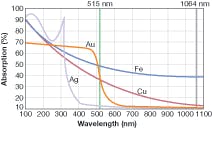
The laser treatment of nonferrous metals such as copper or noble metals such as gold is a challenge for laser processing using conventional lasers working in the near-IR regime. Laser radiation above 1000 nm gets reflected at more than 98%; only a small fraction of the incident power is absorbed. The absorption of laser power at 515 nm, however, is substantially higher (see Fig. 2)-for copper the absorption coefficient is well above 30%, which is favorable for development of a stable manufacturing process.
The 50 W output at 515 nm makes the frequency-doubled thin-disk laser well suited for advanced micromaterials-processing applications in the electronics and semiconductor industries. Because the laser operates in true CW mode, the application of energy is homogeneous and controllable. This characteristic is a major advantage compared to pulsed laser systems, which produce high peak power and low duty cycles. The CW output power of the new laser source can be varied during the welding process, enabling process parameters to be set in real time for highest throughput and quality.
Copper welding in microelectronics
Because the laser was developed within the Joitec research-and-development project for lead-free joining for microelectronics and microsystems-technology devices, most of the initial work addressed copper-copper welding of electronic components. Here, the beam is deflected by a high-speed x-y scanner unit with a large working area; this unit does not increase the spot size of the focused beam on the work piece.
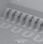
Another application example is solder-free direct welding of copper wires to electronic components such as sensors, relays, and switches (see Fig. 3). Several conditions have to be fulfilled for the finished product; for example, the electrical connection must be robust and insensitive to environmental influences.
Depending on the size of the contact pads and the wires to be welded, the process time is on the order of 5 to 20 ms. Process time should be kept as short as possible to minimize the thermal load on the workpiece. Unlike conventional soldering techniques, high-power-laser welding meets this objective. The resulting mechanical strength of the welded connection is stronger than that of a soldered joint.
Another example is the welding of heat-sensitive electronic or optoelectronic components on the connector pads of printed-circuit (PC) boards. For integrated chips, the contact pins are welded to the contact pad of a PC board. Tests have confirmed that the welding connection is at least as stable as a conventional solder connection, but much easier to control. The precise control of all weld parameters (optical power, time, and spot size) ensures that the thermal load is as low as possible. Therefore, only a limited thermal stress occurs in comparison to conventional techniques.
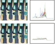
The frequency/intensity distribution of the plasma generated by the welding process can be used to optimize the weld parameters for each spot (see Fig. 4). Combined with shear measurements for the mechanical strength, these measurements serve as the basis for fast and efficient process development.
null
Copper welding for wires or meshes
Direct welding of flatband copper wires or meshes can also be performed to replace cumbersome soldering procedures. Substantially shorter process times and higher shear force on the joints have been achieved because of the large depth of field and small spot sizes. A Gaussian beam profile is required for this application.
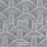
A nonelectronic application is the welding of fine copper meshes used in demanding printing processes such as for passports or money bills (see Fig. 5). Compared to manual soldering procedures, welding delivers not only higher-strength connections, but also the replacement of tedious manual soldering by a reliable automated process. With direct copper welding, the overall process time is reduced by a factor of ten. None of the corrective measures necessary in the manual-soldering procedure are required.
null
Silicon and semiconductor treatment
Initial tests using the 50 W laser for lithographic applications have shown substantially shortened process times compared to frequency-doubled Nd:YAG lasers at 532 nm with conventional power levels around 15 W. For these applications, an excellent beam profile is mandatory to enable the writing of ultrafine structures.
The high CW power is of advantage for many other applications, such as nanopatterning or laser temperature-annealing of silicon. In addition, the laser can be useful for large-screen projection. Unlike with Q-switched green lasers, the beam can be deflected very fast without flicker, allowing projected continuous lines to be moved about quickly on the screen-required in advanced light-show applications.
Other applications include semiconductor and glass manufacturing processes, as well as treatment of dielectric materials. Also, for some processes that currently require UV-emitting lasers, the high-power green laser source is a cost-effective and compact alternative.
GÜNTER HUMMELT is the managing director of ELS Elektronik Laser System, Am Schaubacher Berg 25, 64401 Gross-Bieberau, Germany; e-mail: [email protected]; www.els.de.
