Multicell diode-laser qualification benefits industrial-laser manufacturers
Rigorous techniques adopted from telecom, such as improved manufacturing methods and multicell qualification, permit diode lasers to be confidently deployed across a wide temperature and power range.
TOBY STRITE, VICTOR ROSSIN, MATTHEW PETERS and ERIC ZUCKER
Over the course of the last decade, vendors of telecom-grade diode lasers delivered 25% annual productivity improvements in terms of cost per watt and rated output power-a Moore’s Law-type pace. However, little of this innovation reached industrial customers because the most capable chip houses focused on lucrative, fast-growing telecom markets.
During the five years since the telecom bubble burst, high-end vendors have eagerly diversified into industrial applications. For solid-state and direct-diode laser tools to realize their potential, they must become as reliable as the drill bits, saws, and soldering irons they are slated to replace while offering superior cost of ownership. Extremely bright, telecom-grade diodes are now available at industrial price points, setting new standards for performance and reliability. If industrial-diode technology delivers 25% annual cost-per-watt improvement through technical advances and increased manufacturing efficiency, a productivity-driven boom in diode-pumped solid-state lasers and direct-diode applications is bound to follow.
Laser-diode failure mechanisms
Highly reliable diode-laser products result from stringent efforts to identify and then suppress as many failure mechanisms as possible, followed by equally rigorous efforts to quantify remaining failure modes. Diodes can fail suddenly in a time-dependent or independent fashion, or through gradual degradation. Each signature can have multiple root causes. The most common failure modes include infant failure, catastrophic optical-mirror-damage failure, wear-out, and bulk failure.
Infant failure rates decay rapidly during early operation, as manufacturing defects including metallization voids/cracks, optical coating imperfections, and crystal defects in the active area drive rapid failure. Rigorous burn-in testing at high drive current and ambient temperature is the accepted technique to screen out infant failures. A delicate balance exists such that the overstress must be severe enough to eliminate diodes subject to infant mortality over an economically viable burn-in period, but cannot introduce damage leading to new failure modes. Only highly robust diode lasers meet both criteria.
Catastrophic optical-mirror-damage (COMD) failure is a thermal runaway at the facet region caused by optical absorption. Under normal operation, COMD arises in aluminum gallium indium arsenide (AlGaInAs) devices through facet oxidation that liberates metallic arsenic. Reliable versions of these lasers fully suppress COMD through proprietary facet passivation techniques.
Wear-out failure is a slow degradation present either throughout operation or surfacing late in life. If the degradation rate is constant, failure is defined by a predetermined increase of the drive current required to maintain the beginning-of-life output power. When the wear-out rate is time dependent, quantifying the failure mode is more complex.
Bulk failure is caused by optical absorption triggered by random migration of a crystal defect into a region of high optical field. In essence, this is another form of catastrophic optical damage, only within the diode cavity. Telecom-grade AlGaInAs laser diodes, in which infant and COMD failures are effectively suppressed, have been proven in the lab and field to have low residual bulk failure rates described by:
Here, Fop is the failure rate, and Top, Pop, and Iop are the operating temperature, power, and current intended for the laser-diode deployment. An Arrhenius term scales by an activation energy (EA) with diode p-n junction temperature (Tj). Laser-diode power (P) and current (I) scale exponentially. The multicell testing technique is commonly used to derive the above parameters.
Designing for reliability
Diodes made from AlInGaAs feature the highest demonstrated optical-power density and electrical-to-optical power conversion efficiency (PCE), while covering the 800 to 1000 nm band critical for neodymium (Nd)- and ytterbium (Yb)-based solid-state laser pumping.
The prominence of AlGaInAs is due to its outstanding material quality, design flexibility, and inherent reliability arising from superior-quality GaAs substrates; mature metal-organic chemical-vapor-deposition or molecular-beam-epitaxy growth technologies; lattice-matched AlGaAs waveguide and barrier layers; strained, pseudomorphic InGaAs quantum wells; good n- and p-type dupability; good thermal conductivity, strong III-V bond energies (well in excess of photon energy); and stable, high-quality mirror facets (when properly passivated). Among these many good points, several aspects of device design and processing stand out in the quest for outstanding reliability.
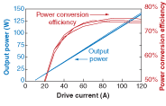
On the device design side, the failure-rate equation reveals that high PCE is critical because of the strong link between failure rate and the device operating current and junction temperature. Operating current is reduced by trading off threshold current and slope efficiency for a specified output power. Junction temperature is reduced by improving waste-heat removal and reducing the total current and voltage for a specified output power. Optimized AlGaAs stoichiometry and doping balance low electrical series resistance with good electrical confinement to reduce carrier leakage, and low optical loss with maximum optical-mode overlap with the gain region.
Several U.S.-based vendors, enabled by funds from the Defense Advanced Research Projects Agency (DARPA; www.darpa.mil) Super High Efficiency Diode Sources (SHEDS) program, have explored and significantly extended the limits of diode-laser efficiency (see Fig. 1).
The best design is unreliable if manufacturing processes are not maintained under constant control. Key processes required for reliability include facet passivation and gold tin (AuSn) soldering of the diode to its heat sink. A passivated facet region ensures a stable-as opposed to a deteriorating-COMD limit. Several methods effectively passivate AlGaInAs facets, while an alternative camp obviates oxidation problems using an “aluminum-free” gallium indium arsenide phosphide (GaInAsP) active region. A well-formed, hard solder joint ensures efficient and uniform heat removal, and permits the diode laser to be power-cycled without degradation.
Predicting reliability
The favored statistical method to predict laser-diode reliability is multicell (MC) testing because it is cost-effective and statistically rigorous. A well-designed MC test yields an empirical laser-reliability model across wide ranges of operating power and device temperature-tantamount to a “user’s manual” for the diode-laser device.
The MC test is a series of parallel lifetime tests on similar devices in which the parameters of the failure-rate equation are systematically varied to determine the independent effect of each on reliability. Because the underlying failure rate of a reliable diode laser is very low, tests are conducted under highly accelerated temperature and drive-current conditions to realize a statistically significant number of failures.
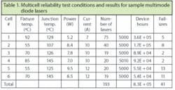
Using JDSU’s 6390 chip (a 100 µm aperture, 910 to 980 nm, junction-side-down multimode diode laser) as an example, 193 devices from four separate wafer runs were loaded onto temperature-controlled test racks after a standard burn-in process. Six test cells were operated at constant current and diode junction temperature for 5000 hours each. Cells with lower expected failure rates include more devices to ensure statistically relevant failure counts. An identical sudden failure signature was observed in every cell, indicating high stress conditions do not engender new failure modes. No wear-out was observed in any cell (see Table 1).
The MC test design indexes three junction temperatures (Tj approximately 107°C, 126°C, 145°C) against three drive currents (I = 7 A, 10 A, 12 A), but the results indicate power is a stronger accelerant than current. For example, cells 5 and 6 (I = 12 A) illustrate that the lower diode efficiency at higher junction temperature results in a reduced failure rate-a result echoed when comparing cells 2, 3, and 4. The failure rate showed a slight decrease during the MC test, suggesting failures are not purely random in time.
The MC data were analyzed using the commonly accepted maximum-likelihood method. An exponential failure distribution function neglecting current acceleration (m = 0 in the failure-rate equation) provides an excellent fit. The Arrhenius activation energy (EA= 0.41 eV) falls comfortably within the range commonly observed in telecom-grade AlGaInAs diodes, lending confidence to the data and analysis. A strong exponential power acceleration (n = 5.7) confirms optical power as the key accelerant. At the 6.5 W rated operating condition with a heat-sink temperature of 35°C, a mean time between failures (MTBF) of 690,000 hours is derived within a 60% statistical confidence level.
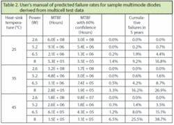
The key advantage of the MC approach is the ability to predict reliability across a wide range of conditions, permitting customers with varying reliability requirements and operating environments to confidently deploy the diode laser (see Table 2). Reliability-conscious customers may derate power by 20% to 5.2 W to enjoy a three-million-hour MTBF. Customers with reduced reliability demands can operate at 8 W while still achieving an MTBF of 190,000 hours.
Devices can also be reliably deployed at elevated temperature to reduce cooling system requirements. Robust distributed pump architectures using multiple 6390 laser diodes in electrical series with 10% to 20% redundancy achieve five-year continuous usage with better than 99% confidence of no pump-related system failure. Such an up-time guarantee is unprecedented in the industrial-laser marketplace. Clearly, ultrareliable diode-laser technology is a significant enabler to increase the penetration of solid-state and fiber lasers on the factory floor.
TOBY STRITE is manager of high-power laser marketing, VICTOR ROSSIN and MATTHEW PETERS are senior development engineers, and ERIC ZUCKER is manager of high-power laser product development in the High Power Lasers Business Unit of JDS Uniphase, 430 N. McCarthy Blvd., Milpitas, CA 95035; e-mail: [email protected].


