World’s smallest silicon LED enables nanoscale holographic microscope
A team at the Singapore-MIT Alliance for Research and Technology (SMART) has developed the world’s smallest silicon LED (see video). It’s smaller than a wavelength of light, but emits as much intensity as LEDs that are much larger. The researchers’ intent was to create a highly efficient, low-cost LED that operates in the near-infrared (near-IR) range.
“We achieved this with a new silicon device structure to improve its efficiency emitting light in the near-IR range,” says Rajeev Ram, a professor of electrical engineering at Massachusetts Institute of Technology (MIT; Cambridge, MA) and a principal investigator with the SMART Critical Analytics for Manufacturing Personalized-Medicines (CAMP) and the MIT Disruptive and Sustainable Technology for Agricultural Precision (DiSTAP).
Specifically, the team used a technique called silicon nanostructuring, “in which we created nanoscale features on the surface of the silicon material to improve its light emission properties,” he says.
The silicon LED they developed has several advantages over traditional LEDs. First, it’s made of silicon, a widely used semiconductor material, so it can be built using existing manufacturing processes, which makes it highly scalable and cost-effective to produce. It also leverages the precision of silicon manufacturing to build a device smaller than the wavelength of light.
“This makes the light emission spatially coherent—light waves at different locations have synchronized peaks and troughs,” says Zheng Li, a research scientist at MIT. “And it’s useful for applications using wave interference, such as holography.”
Holographic microscope
Given the extremely small size of the silicon LED, the researchers used it to create a compact, holographic microscope that can be used with existing smartphone cameras.
Their holographic microscope, which the researchers say is the world’s smallest, features two components: the team’s nanoscale silicon LED and a silicon-based image sensor like those found in mobile phones.
“We were able to create holographic images of cells using the microscope, demonstrating the potential of our silicon LED for use in biomedical imaging and diagnostics,” Ram says.
“The coherent IR light from the LED passes through the object to be imaged,” Ram explains. “This object changes the synchronization of the light waves at different points along the beam, which gives rise to a pattern of interference recorded by the image sensor. Computational processing of the recorded interference pattern, or digital hologram, reconstructs an image of the microscopic object.”
This is an important breakthrough in the field of optoelectronics, he notes, with significant implications for a range of applications in sensing and imaging. Silicon nanostructuring can improve the efficiency of light emission, and may also pave the way for the development of new and improved optical systems.
Compact design is key
The silicon LED and holographic microscope both offer several advantages over existing technologies. Their compact design is one. Since the LED is much smaller than conventional LEDs, it increases the coherence of emitted light. “This allows us to make large, dense arrays of these LEDs, which will enable higher-resolution imaging systems,” Li says.
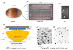
GlobalFoundries Singapore is already fabricating the LED alongside millions of transistor components on 300 mm wafers in a facility capable of high-volume manufacturing (see Fig. 1).
Importantly, the holographic microscope is compatible with existing devices and is easy to integrate into mobile phone cameras. This makes it possible to capture high-resolution images of biological samples in remote or resource-limited areas where larger, more expensive equipment isn’t typically available.
The LED and microscope offer new possibilities for producing 3D images of cells, tissues, and other biological samples, which could provide important insights into their structure and function (see Fig. 2).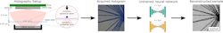
“Our holographic microscope can also be used for point-of-care testing, because it can be easily integrated into mobile phone platforms, which makes it a cost-effective and accessible diagnostic tool,” he says, citing other applications such as imaging of plant tissues in agritech or precision agriculture to optimize crop health and yield, and imaging of living human cells for cell therapy. Environmental monitoring and sensing are other possibilities, which could help researchers detect and monitor pollutants in water or air, or to monitor the growth of microorganisms in environmental samples.
What’s next?
The silicon LED and holographic microscope are advancing, thanks to the team’s ongoing research. “While our new silicon LED is already smaller and brighter than previous silicon LEDs, its efficiency can still be improved,” Ram says. “Future research could focus on optimizing the LED's design and fabrication process to increase its efficiency and brightness.”
Development of new holographic imaging techniques are also in the works. The holographic microscope can already create high-resolution, 3D images of biological samples, but future research can go farther by exploring a single-chip version of the holographic microscope where the LEDs and image sensor are on the same chip and the hologram is created from light reflected from the object.
About the Author

Justine Murphy
Multimedia Director, Digital Infrastructure
Justine Murphy is the multimedia director for Endeavor Business Media's Digital Infrastructure Group. She is a multiple award-winning writer and editor with more 20 years of experience in newspaper publishing as well as public relations, marketing, and communications. For nearly 10 years, she has covered all facets of the optics and photonics industry as an editor, writer, web news anchor, and podcast host for an internationally reaching magazine publishing company. Her work has earned accolades from the New England Press Association as well as the SIIA/Jesse H. Neal Awards. She received a B.A. from the Massachusetts College of Liberal Arts.