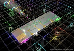
On-chip quantum light source generates entanglement
Leibniz University Hannover (Germany) researchers recently teamed up with colleagues from the University of Twente and startup QuiX Quantum (both in Enschede, Netherlands) to address one of the most fundamental roadblocks holding up quantum technologies: a lack of scalability.
Until now, on-chip-based quantum photonic systems for processing or communications were driven by an external bulky laser system, typically the size of a shoebox, sitting on a shelf beside the photonic quantum chip. Quite undesirably, this limits scalability and applications.
“Quantum communications need energy-efficient, fully chip-scale quantum sources to scalably create many transceivers for quantum internet nodes,” says Michael Kues, head of the Institute of Photonics at Leibniz University Hannover. “For quantum computation, the envisioned quantum accelerators need to be efficient and adhere to data center formats.”
To address scalability, the team designed an electrically excited laser-integrated photonic quantum light source right onto a chip to emit photons that can be used as frequency-entangled qubit states (see figure and video).
Designing an on-chip quantum light source
How did the researchers pull off this design? By putting a laser cavity, a tunable noise-suppression filter (microrings/waveguides), and a parametric quantum source of entangled photons onto a chip.
Intriguingly, their hybrid chip design combines two different semiconductor materials: an indium phosphide laser’s light is passed along to the rest of the silicon nitride chip using waveguides and three nonlinear microring resonators, which act as a noise-suppression filter. As the light exits the third microring, a pair of entangled photons are generated.
Focusing on designing a filter to address qubits’ susceptibility to noise paid off because the researchers say their chip is completely devoid of noise. “One of the biggest challenges along the way,” Kues says, “was integrating the filter between the gain medium and the parametric source within the integrated device.”
Their design also enables shrinking the quantum light source size by a factor of more than 1000—without cryogenic systems.
Perhaps the coolest aspect of this work is the compactness of the chip (smaller than a one-euro coin), which makes it easy to handle. “It contains everything previously on a big table—and generates near-perfect entangled states,” Kues says. “Users just need to switch it on. There are no extra components or stability issues, and no struggle to couple the laser light for hours.”
The chip demonstrates “remarkable efficiencies and state qualities required for quantum computers or the quantum internet,” he adds.
Now that the researchers have demonstrated the stability of their integrated and scalable quantum source, “the next step is to use the source in applications such as quantum communications or scale it further for processing applications,” says Kues. “Another challenge is to improve its fabrication—hybrid chip combination—to allow mass producibility.”
FURTHER READING
H. Mahmudlu et al., Nat. Photon. (2023); https://doi.org/10.1038/s41566-023-01193-1.
About the Author
Sally Cole Johnson
Editor in Chief
Sally Cole Johnson, Laser Focus World’s editor in chief, is a science and technology journalist who specializes in physics and semiconductors.

