VCSELs: From telecom to the metaverse
If we could pay tribute to just one critical technology that enables today’s nearly constant virtual connectedness, little laser sources would be high on the list. In particular, one little laser technology, vertical-cavity surface-emitting lasers (VCSELs; a term coined in 1987), evolved over several decades to enable the high-speed networks that keep us connected. Today, applications are far from telecom.
In 1977, Bell Labs researcher Kinichi Iga first conceived of a tiny monolithic semiconductor laser diode as a low-cost alternative to edge-emitting lasers in optical fiber transmission. The diode would emit vertically, perpendicular to the surface of a thin film, which could be cheaply fabricated at volume via large wafers. Iga’s 1980 prototype used a 6-µm-thick cavity etched on a gallium-indium-arsenide-phosphide (GaInAsP) thin film, but it suffered from high optical loss. He kept working on the idea persistently; other researchers caught the fever.1
It wasn’t until 1996 that Honeywell International (Richardson, TX) launched the first commercial VCSEL, an 850 nm GaAs proton-implanted diode for room-temperature operation in fiber-optic links less than 300 m.2 The 850 nm GaAs VCSEL soon became a ubiquitous, critical component in the evolution of widespread fiber-optic networks for data communications. The quick success of VCSELs was due to their inherently monolithic design, which enables cost-efficient volume fabrication, high reliability, high beam quality, fast modulation bandwidth, low power requirements, and scalability via arrays. Furthermore, the incorporation of distributed Bragg reflectors and microcavity designs have enabled low power density thresholds, making VCSELs very power-efficient light sources.3
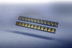
Today, the biggest application for VCSELs is 3D sensing for face identification in mobile phones. But it took some novel advances to get there. Single VCSELs are too low-power for consumer devices, but are scalable by fabricating an array of VCSELs directly on a wafer, and collimated with lenses to magnify the power to the single-watt range. According to Andre Wong, 3D sensing vice president at VCSEL manufacturer Lumentum (San Jose, CA), large arrays of 2D VCSEL chips were originally fabricated on 4-in. wafers for use in datacom devices. But to make sense economically in consumer devices, VCSEL foundries had to make the jump to 6-in. wafers, a wafer size used for cell-phone fabrication since the 1990s. By fabricating more VCSEL arrays per wafer, VCSEL technology could take advantage of well-established GaAs 6-in. wafer fab technology. Around 2015, the 6-in. fab platform began to enable higher economies of scale for VCSELs as well as for ease in volume testing prior to wafer dicing (see Fig. 1).
“The 6-inch wafer enabled Gen 1, first generation VCSEL products, including eye-tracking, gesture recognition, and depth sensing,” says Wong. “Today’s technology advances: multi-junction stacking, multilayer metal, and back-side emission will enable Gen 2 VCSEL products like automotive lidar, AR/VR headsets, and health monitoring.”
Multi-junction advantages
Early VCSELs had a single p-n junction, which limited sensing range and output power, usually <10 mW for a single device. Stacking several single-junction VCSELs enables multi-junction arrays, which achieve higher peak optical power densities and efficiency, and simplifies the driver and package design. Multi-junction designs allow VCSELs to sense further, enabling longer-range applications like automotive LiDAR. For similar reasons, multi-junction VCSELs offer better short-range 3D sensing due to improved power output and more complex integrated optics capabilities.
Multi-junction technology just launched within the past few years, with products in advanced consumer, automotive LiDAR, and other 3D sensing applications recently commercialized. In October, Lumentum announced an industry-first three-junction VCSEL array that enables time-of-flight (ToF) biometric 3D sensing in cellphone security. The 10-W flood illuminator incorporates a high-performance three-junction VCSEL array, which enables customers to choose three different illumination fields: 60 × 45, 72 × 58, or an even wider 110 × 85 degrees, which can capture more information at higher power and higher efficiency without losing eye-safe functionality. The three-junction VCSEL array will also be useful in emerging industrial and consumer artificial intelligence of things (AIoT) applications, where the two technologies converge in areas like testing and fabrication. Subsequently, Lumentum researchers demonstrated high-performance five- and six-junction VCSEL arrays, the first trick of the kind in the industry.
Addressability
Early LiDAR systems used mechanical beam scanning, with spinning laser modules that were bulky, impractical, and too delicate for automotive applications. Multi-junction VCSEL arrays on a chip have achieved the range necessary for LiDAR, in addition to being robust, miniature, and cheap, but typical interconnect schemes don’t support 3D sensing that can adaptively illuminate various regions of interest (ROI), a feature called addressability, or smart illumination. Defined as the ability to control and independently illuminate different rows or segments of an array, smart illumination is required for VCSEL-powered automotive LiDAR to directly image the scene, control what’s illuminated, and reduce power use. With breakthroughs in multilayer metals and driver electronics, Lumentum announced in November 2021 the launch of the first high-performance 1D and 2D addressable VCSEL arrays for automotive, consumer, and industrial LiDAR and 3D sensing applications. The addressable arrays emit at 905 nm and 940 nm, opening up the potential in both short- and long-range LiDAR.
"On-chip array addressability can eliminate the need for mechanical beam scanning, which opens a new world of possibilities for lidar in autonomous vehicles and other emerging 3D sensing applications," says Matt Everett, product line director of 3D Sensing at Lumentum.
Longer wavelengths
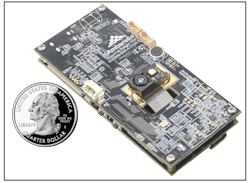
While 850 nm VCSELs helped launch the mobile revolution, the 940 nm VCSEL array has likewise been a workhorse since 2014; it’s easily paired with existing CMOS-based GaAs sensors. Near-infrared (NIR) is the wavelength at which atmospheric moisture absorbs sunlight, making 940 nm well suited for outdoor apps. And VCSEL R&D is expanding into ever-longer wavelengths. In March 2022, Lumentum partnered with germanium-silicon (GeSi) tech leader Artilux (Hsinchu, Taiwan) to demonstrate the world’s first NIR/shortwave-IR (SWIR) sensing platform for consumer true wireless stereo (TWS) wearables (see Figs. 2 and 3). The NIR/SWIR optical sensing platform combines Lumentum’s 940- and 1380-nm VCSEL arrays with Artilux’s CMOS-based GeSi sensors, creating an all-in-one module with a compact form factor and ultralow power requirements. The future TWS earbuds will enable skin detection inside the ear to deliver seamless sound while preserving battery life. SWIR at 1380 nm is magnitudes more eye-safe than other wavelengths, penetrating more deeply into tissue without damage. The NIR/SWIR combination is ideal for automotive LiDAR, medical imaging of live tissue, and consumer 3D sensing in cell phones and wearables.
Research continues pushing the bounds of what’s possible, with 2 µm (ideal for gas sensing) not far behind, as well as at shorter wavelengths. Researchers in China recently demonstrated tunable VCSELs operating in the ultraviolet A (UVA) region of the spectrum from 376 to 409 nm with threshold power densities on the order of 400 kW/cm2, among the lowest values claimed, while Nichia has reported success with 1000 hours of continuous operation of blue VCSELs.4 While the commercial realization of blue and UV VCSELs may take some time, their potential in applications like full-color picoprojectors and retinal scanning is exciting.
As well as breaking records for peak optical power densities and efficiencies, VCSELs are also reliable. Lumentum claims to have shipped over a billion VCSEL arrays in the past several years with no failures. With that kind of progress, the next generation of VCSELs will no doubt soon find use in AR/VR devices—the linchpin in the development of the metaverse.
“The number of applications is just endless,” says Wong. “We started out with mobile phones, migrated into automotive LiDAR and in-cabin, and we’re now seeing applications in access control, machine vision, occupancy monitoring, and payment kiosks. With longer wavelengths, we’ll have the AR/VR headset market and healthcare. Every few months, there’s another use for VCSELs.”
Tomorrow’s telecom
While tomorrow’s metaverse and IoT applications are a far cry from their telecom origins, VCSELs are still involved in future-facing telecom initiatives, too. Datacenters and wireless operators are pushing toward 200G and even 800G hyperscale connectivity, in which VCSELs will play an important role in lowering cost, latency, and power requirements.
Datacenters today typically deploy optical modules using 4x25G non-return-to-zero (NRZ) links to achieve 100G network speeds, which require analog clock and data recovery (CDR) chipsets. The next data rate milestones for datacenters are 200, 400, and 800G using optical interconnects and CDR technology that can accommodate “pulse amplitude modulation level 4” (PAM4) signaling.
However, traditional PAM4 links require digital signal processing technology, which uses more power and therefore increases operating costs. To address this, semiconductor supplier Semtech (Camarillo, CA) recently introduced the Tri-Edge CDR platform for PAM4 applications ranging from data centers to 5G wireless optical communications. The Tri-Edge CDR chipset uses analog technology to enable a range of lasers, including VCSELs, directly modulated lasers, and electro-absorption modulated lasers, in a low-power, low-latency solution, achieving <500 ps of absolute latency and near-zero latency variation. Such innovations in integrated chip technology will keep us streaming at screaming speeds for decades to come.ACKNOWLEDGMENT
Tri-Edge is a registered trademark of Semtech.
REFERENCES
1. K. Iga, Jap. Journ. Appl. Phys., 47, 1 (2008); https://doi.org/10.1143/jjap.47.1.
2. J. Tatum et al., Proc. SPIE, 3946 (May 2000); https://doi.org/10.1117/12.384359.
4. H.-T. Chen et al., Photonics, 9, 107 (2022); https://doi.org/10.3390/photonics9020107.
4. Y. Mei et al., Fund. Research, 1, 6 (2021); https://doi.org/10.1016/j.fmre.2021.11.001.
About the Author

Valerie Coffey-Rosich
Contributing Editor
Valerie Coffey-Rosich is a freelance science and technology writer and editor and a contributing editor for Laser Focus World; she previously served as an Associate Technical Editor (2000-2003) and a Senior Technical Editor (2007-2008) for Laser Focus World.
Valerie holds a BS in physics from the University of Nevada, Reno, and an MA in astronomy from Boston University. She specializes in editing and writing about optics, photonics, astronomy, and physics in academic, reference, and business-to-business publications. In addition to Laser Focus World, her work has appeared online and in print for clients such as the American Institute of Physics, American Heritage Dictionary, BioPhotonics, Encyclopedia Britannica, EuroPhotonics, the Optical Society of America, Photonics Focus, Photonics Spectra, Sky & Telescope, and many others. She is based in Palm Springs, California.