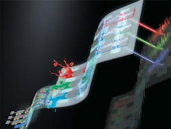
Colloidal quantum dot laser research overcomes challenges
In a new review article published in the journal Nature Photonics, scientists at Los Alamos National Laboratory (LANL; Los Alamos, NM) assess the status of research into colloidal quantum dot lasers with a focus on prospective electrically pumped devices, or laser diodes. The review analyzes the challenges for realizing lasing with electrical excitation, discusses approaches to overcome them, and surveys recent advances toward this objective.
“Colloidal quantum dot lasers have tremendous potential in a range of applications, including integrated optical circuits, wearable technologies, lab-on-a-chip devices, and advanced medical imaging and diagnostics,” says Victor Klimov, a senior researcher in the Chemistry division at LANL and lead author of the Nature Photonics article. “These solution-processed quantum dot laser diodes present unique challenges, which we’re making good progress in overcoming.”
Laser diodes usually employ ultrathin semiconductor films, or quantum wells, grown via vacuum-based layer-by-layer atomic deposition. While allowing for exquisite control of the material’s properties, this growth method is highly demanding and requires a cleanroom environment. In addition, it is restricted to a fairly small number of mutually compatible materials used as a lasing medium and an underlying substrate. Specifically, compatibility issues greatly complicate integration of existing semiconductor lasers with standard silicon-based microelectronics.
“These problems can, in principle, be resolved with inexpensive solution-processable light emitters,” Klimov says. “In particular, an attractive alternative to standard quantum wells is semiconductor particles prepared via bench-top colloidal chemistry.”
Colloidal quantum dots can be synthesized in bulk quantities in a standard wet-chemistry lab using inexpensive, readily available precursors. Further, they can be combined with virtually any substrate that would resolve the issue of compatibility with silicon microelectronics and open new areas of applications not accessible with traditional laser diodes.
There are also additional advantages derived from the unique quantum nature of colloidal nanocrystals. In particular, due to their ultrasmall sizes, their emission wavelength can be readily tuned by varying nanocrystal dimensions. This powerful capability could enable laser diodes with an ultra-wide range of accessible colors. Further, the discrete structure of quantum-dot atomic-like states inhibits thermal depopulation of the lowest-energy emitting states and thereby reduces lasing thresholds and improves temperature stability of a lasing device.
“Despite these potential benefits, the colloidal quantum dots are difficult lasing materials,” Klimov says. “High-quality nanocrystals have been available since the early ‘90s. However, they would not lase until around 2000, when our team at Los Alamos demonstrated for the first time the effect of light amplification with cadmium selenide nanocrystals.”
The key to this demonstration was two important discoveries made at LANL. One was the realization that optical gain relies not on single excitons (as in a standard light emission process), but on biexcitons and other states of higher multiplicity. The other identified challenge was that the primary deactivation channel of biexciton states was very fast nonradiative Auger recombination whereby biexcitons generate heat instead of light.
To resolve these challenges, LANL researchers utilized densely packed quantum dot solids, which allowed them to boost the rate of stimulated emission so it could outpace Auger decay. Further, they employed very short (about 100 fs) pulses to populate quantum dots with biexcitons before they had a chance to decay via the Auger process. This approach produced a long-awaited result—the realization of amplified spontaneous emission, proof-of-principle for colloidal quantum dot lasing.
Auger recombination still represents a major obstacle for the realization of technologically viable quantum dot lasers. Another serious challenge is the development of practical devices that can sustain ultra-high current densities of hundreds of amperes per centimeter squared required for lasing. The realization of such structures is greatly complicated by poor charge-transport properties of granular quantum dot solids and high resistivity of solution-processed charge-transport layers. As a result, devices are quickly overheated at high current densities and eventually fail due to heat-induced breakdown.
To resolve the thermal damage problem, LANL developed a new device architecture in which current flow was restricted to a small area of 50 × 300 µm. This current-focusing approach boosts current density and simultaneously reduces the heat generation volume and improves heat exchange with the environment. An additional trick was to deliver carriers in short bursts of current between which the active volume had a chance to dump heat into a surrounding medium.
These measures allowed for boosting the current densities to unprecedented levels of about 1000 amperes per square centimeter, more than a hundred-fold enhancement compared to previous records. This was sufficient to achieve broadband optical gain capable of sustaining lasing across a wide range of wavelengths spanning from red to yellow with a single quantum dot sample.
Another challenge is incorporation of an optical resonator so as it does not disrupt charge injection pathways and, at the same time, maintains lasing despite the presence of “optically lossy” charge transport layers. This problem also has been recently resolved by LANL researchers.
In particular, they applied an interesting approach wherein an optical resonator was prepared as a periodic grating engraved into a layer serving as an electron injector. In this way, they preserved a standard architecture of a light-emitting diode (LED), but endowed it with an additional function of lasing device. The developed dual-function structures performed as a standard LED operating under electrical pumping and a laser activated optically.
The final step is to combine all of these strategies in a single device capable of lasing with electrical excitation.
Heeyoung Jung and Namyoung Ahn, also of LANL’s Chemistry division, are coauthors of the Nature Photonics article.